Golden Cove – Architectural Deep Dive
Golden Cove = Performance Core
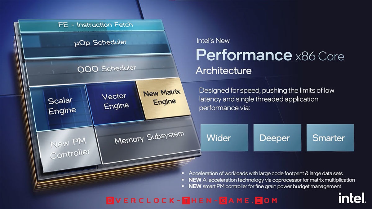
Now we move to the area that everyone will care more about, the Performance Core, codenamed “Golden Core”. Once again Intel is attempting to capture several markets with one design. The Performance Core goals are speed, single-threaded performance and low latency. As data and workloads are growing Intel designed the Performance Cores to be able to bring in more data and complete work on that data as effectively as possible. Although single-threaded performance is one of Intel's goals, the Golden Cove microarchitecture does support Hyper-Threading (SMT) unlike the Gracemont Cores. Golden Cove Performance x86 Core is broken down into areas, with those being: Instuction Fetch, uOP Scheduler, OOO Scheduler, Scalar Engine, Vector Engine, New Matrix Engine, New PM Controller, Memory Subsystem. So as we can see the Performance Core differs a bit from the Efficient Core.
Front End
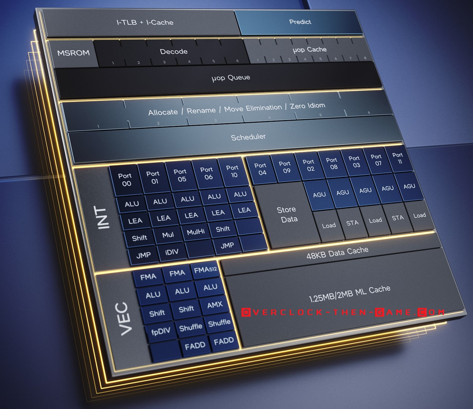
Golden Core contains 32KB in L1 Instruction Cache, but the L1 Data Cache was increased to 48KB. The Length Decoder was increased to 32Bytes from 16Bytes found in the 11th Gen (Rocket Lake). As far as I am aware the Instruction Length Decoder is not in the Instruction Cache as found in the Gracemont Core. The branch target was increased as well to 12K branch targets which are up from 5K in the previous 11th Generation. Intel says that their branch predictor can hide many of the instruction cache misses, which could cause latency. Intel also claims that their branch predictor uses a machine learning algorithmic which can cause the branch predictor to grow or shrink its size and by size I believe Intel means its capacity\entries. Supposedly for programs that aren’t that large in size\code, the branch predictor can save power by turning off some of its area\capacity; however it can power up and expand its size when larger code is sent to the core. Intel seems to have set some ambitious goals with Alder Lake. Little things like this is what most people would look over, but it appears Intel is capable and feels comfortable talking about it.
Feeding the Beast
Intel has added two decoders that can output 6 micro-ops to the micro-ops cache (11th Gen could output 4). The uops cache can also hold 4K of data. The micro-ops cache can output 8 uops per cycle to the uops queue. From my understanding the uops queue can hold 72 entries per thread (SMT) and if it’s a single thread it can hold 144 entries. That is a 157% increase for SMT (Hyper-Threading) and a 414% increase for single-thread when compared to my 1st Generation CPU. The goal for Intel is to increase the hit rate to prevent long and wasted cycles that could mean transferring more data to and from the system memory. The out-of-order engine can allocate 6 uops and the reorder buffer can hold a staggering 512 entries which is also a 300% increase over my 1st Generation CPU. The goal in this case is to ensure that workloads can be scheduled accordingly, especially if there are no dependencies. Intel wasn’t joking when they said Alder Lake had a deeper out of order engine. To make all this work Intel uses their proprietary interconnect that allows the cores and core-memory subsystem to connect to the IMC.
Alder Lake Performance x86
Intel added an extra INT EU which pushes Alder Lake Execution Units to 5 for INT or none FP\Vector workloads. The extra EU contains the ALU and LEA only. The LEA is on all INT EUs and only takes 1 cycle for arithmetic calculations. LEA can also be used to quickly move information such as an address to a register and according to Intel, scaled operations all within a single cycle. Previously ADD operations were completed with the FMA units and took 4 cycles. For the Floating Points\Vector EUs Intel added two FADD (Fast Adders) on Ports 1 & 5. Intel claims that it only takes 3 cycles to complete in comparisons to FMA on the previous 11th Generation uarch (Rocket Lake) which took 4 to 6 cycles to complete depending on the port being used. Intel added an extra AGU Load EU pushing Alder Lake to 3 load ports (1 extra over the 11th Generation). There are a total of 12 Execution Units (up from 10 EUs on 11th Gen Rocket Lake) which means that if all of the Performance Cores are being utilized you can have up to 96 EUs being used at once across all 8 cores. If Intel has away for the Gracemont Efficient Cores to be used effectively with the Performance Cores for the same workloads then you could possibly have up to 232 EUs being used at once. In most cases they would be running different types of workloads, but Alder Lake is appearing to be a workhouse. The AVX-512 Instruction Set is supported with Alder Lake’s Performance Cores, but onlt if the Efficient Cores are disabled and the motherboard OEM supports\allows ASVX-512. AVX-512 will be available for the Enterprise\Server markets.

P-Core Memory Subsystem
Intel has decreased the latency even further when compared the 11th Gen Rocket Lake. Another difference between the Enterprise market and Consumer market is the L2 Cache size. Enterprise will get 2MB L2 Cache while the consumer market will only get 1.25MB Cache (my 1st Generation only has 256KB L2 Cache). That’s not too bad I suppose since the Enterprise markets will obviously need more performance and data throughput than the typical gamer sitting at home running synthetic benchmarks and games. Intel has tailored the L2 Cache to work in conjunction with the prefix engine and more than likely the branch prediction (front) engine so that the L2 Cache will hopefully know, by observing the data flowing into the cache, if more data instructions will need to be pulled from the system memory. This way the CPU won’t get stalled waiting for data if the L2 Cache can go ahead and fetch the data before it is needed. Alder Lake supports 9.5MB up to 14MBs L2 Cache. That is, 1.25MB for each Performance Core and 2MBs for each Efficient (Gracemont) Core. So for the i9-12900K \ KF (8 P-Cores + 8 E Cores) that would be 1.25MBs x 8 (P-Cores) = 10MBs L2 Cache for the Performance Cores. The Efficient Cores in two clusters (x4 Gracemont Cores) share 2MBs for a total of 4MBs L2 Cache. So that would be 2MBs x 2 (E Core Clusters) = 4MBs L2 Cache. Therefore the total L2 cache for the Core i9-12900 K \ KF would be (10MBs + 4MBs) 14MBs L2 Cache.
Alder Lake vs Rocket Lake
This comparison is much better than the 2015 Skylake comparison earlier with the Gracemont-Core. Intel is claiming that their 12th Generation “Alder Lake” Performance-Core is 19% faster than their previous 11th Generation “Rocket Lake”. This probably means that Alder Lake is trillions of times faster than my 1st Generation “Westemere”, especially the “Bloomfield” CPUs.