Alder Lake-S Review
Update: 11-26-2021 - L3 Latency * P-Core BW Results Updated
Introduction
After running Intel’s X58 & 1st Generation CPU for over a decade I have finally decided to upgrade to Intel’s latest and greatest, the 12th Generation Alder Lake-S CPU. There had been plenty of leaks and information leading up to Alder Lake formal reveal, but nothing was official. Intel’s Alder Lake was officially launched on October 27th 2021 and Intel also allowed pre-orders to begin. Alder Lake was officially released on November 4th 2021. Now with official information coming from Intel including the price, specifications, overclocking information and performance numbers; there was plenty to look forward to. Intel revealed that six Alder Lake CPUs would be released on their 10nm cores along with DDR5. In addition to those 6 CPUs for the consumer desktop segment there will be approximately 60 CPUs released across the entire Alder Lake CPU stack for different industries. More than 10 years ago I felt as if I had the cutting edge in technology. My Intel X58 platform included tech such as USB 3.0, SATA 3 & SATA6 ports, dual PCIe 2.0 (x16) slots, one PCIe 2.0 (x4), hardware & software RAID 0, 1, 5 &10, Triple Channel DDR3 1866Mhz+, eSATA 3.0, x2 FireWire and all other types of cool tech during that era. Throughout this article you will notice that I will make comparisons to my Intel 1st Generation CPU as a reference. Looking at the 12th Generation “Alder Lake” CPU and the Z690 chipset more than a decade later we see DDR4-3200Mhz & DDR5-4800Mhz supported, PCIe 5.0 (x16) & PCIe 4.0 (x4) connected directly to the CPU. My 1st Gen microarchitecture only supported DRAM (DDR3) connected directly to the CPU. Other nice 12th Gen technology includes M.2 slots, USB 3, but not the same USB 3 that my X58 motherboard used, Intel’s Z690 boards supports USB3 5G, 10G and 20G. So for me personally this should be a massive upgrade since I have skipped so many releases from both Intel and AMD. Intel’s Alder Lake-S has grabbed my attention and I am excited about the new microarchitecture. Unlike previous microarchitectures from Intel, Alder Lake is taking a page from ARM’s “big.LITTLE” configuration setup. Alder Lake contains larger P (Performance) Cores and smaller E (Efficient) Cores. Windows 11 will be required to take full advantage of Alder Lake’s P-Cores and E-Cores, but I will speak more on that later. It’s amazing to learn and see how Intel’s microarchitecture will perform with a hybrid design. For those who haven’t been following Intel and all of the news over the past several years I’ll try my best to get you up to speed quickly.
Alder Lake-S YouTube Video
Intel 10nm & Delays
For roughly a decade Intel’s proven “Tick-Tock” model worked well which allowed Intel to create a new microarchitecture on existing fabrications before ramping up a smaller node. All good things must come to an end right? Well it did come to an end and in early 2016 Intel replaced the “Tick-Tock” model and revealed a new model called the “Process-Architecture-Optimization”. In 2016 Intel was officially one year behind with their 10nm release and was still using the 14nm architecture, which was also delayed by roughly a year in late 2014. So from 2014 to 2021 consumers have seen Intel optimize their micro-architectures based on the 14nm fabrication (Skylake) using the “Process-Architecture-Optimization” model. Most recently in 2021 Intel has revived their “Tick-Tock” strategy; however it is safe to say that Intel will be continuing their “Process-Architecture-Optimization” model as well. Intel’s 10nm ramping didn’t go as planned in 2016 due to yield defects and other fabrication issues surrounding the 10nm node until around Q3 2018. In 2018 Intel finally released their first 10nm CPU (Cannon Lake), but it was only a 2 Core \ 4 Thread mobile CPU with a TDP of 15Watts. The operating frequency was 2.20GHz and boosted to only 3.20GHz. That’s not much for being roughly 3 years late to the market.
AMD Is Rising & Intel Nodes Renamed
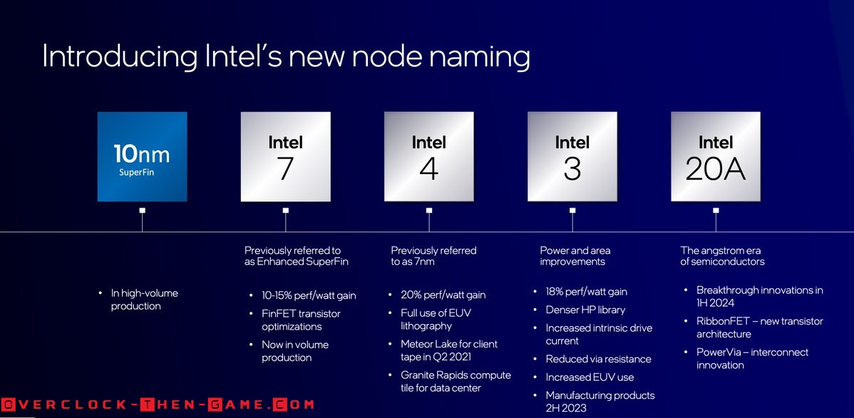
While Intel fell behind with their smaller node (10nm) fabrication this has given AMD plenty of time to catch up with the help of TSMC. AMD has been working on interesting technology over the years ranging from multi-chip modules to Infinity fabric and most recently V-Cache with their Ryzen, Threadripper and Epyc brands. AMD has also regained market share and has overtaken Intel in stock market price. Intel’s node naming scheme has been changed as well. Intel has noticed that consumers have taken precedence in the naming schemes for nodes (i.e 14nm vs 10nm vs 7nm vs 5nm), while leaving out other important details within microarchitecture & process specs for the fabrications. This is also due to the fact that other industry leaders such as Samsung & TSMC etc. have been using different metrics to name their fabrications while Intel has continued to follow the traditional metrics for naming their nodes. Consumers just believe smaller is better when there are many more things to consider in the equation.
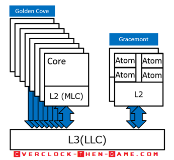
Alder Lake Cove’s and Mont’s
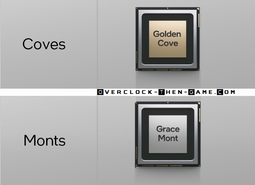
Prior to Alder Lake Intel released their first “Hybrid Technology” based on the “Lakefield” 10nm processor. Lakefield contained 10nm “Sunny Coves” for performance related workloads. In addition to the Lakefield Sunny Cove uarch Intel had “efficient” 10nm “Tremont Cores” as well. This was Intel’s first attempt using their “Hybrid Technology” rollout which was only available on the mobile platforms. Alder Lake is Intel’s very first Desktop CPU to use their Hybrid Technology. Intel's' Alder Lake microarchitecture contains Coves (Performance Cores) and Monts (Efficient Cores). I believe it is a safe bet to conclude that Monts means “Mountains” at this point. The Performance (P)-Cores in this case are the “Golden Cove” CPU uarch (CPU micro-architecture) and the Efficient (E)-Cores are the “Gracemont” uarch. The Golden Coves (Performance) Cores contain Hyper Threading capabilities and are the high performance work horses that we expect. However, on the other hand we have Gracemont (Efficient) Cores which lacks Hyper-Threading, but has been designed for throughput for light background tasks in many cases. This should allow the CPU to use as little power as possible when you aren’t taking full advantage of Alder Lake CPU performance. The 12th Generation Alder Lake processor uses Intel's LGA1700 socket which means that it has 500 more pins than the previous socket (LGA 1200 - 11th Gen Rocket Lake). Intel is known to ensure that their sockets stay roughly the same and that has been the case over the years, however a major redesign was in order for the Alder Lake CPU packaging and the LGA socket. This would make previously released CPU coolers obsolete in some cases for various reasons; however some manufactures will be offering upgradable brackets that will allow current LGA1200 CPU cooling solutions to be compatible with Alder Lake’s LGA 1700 socket. Some motherboard manufactures have both the LGA1200 and LGA1700 cutouts on the motherboard that will allow LGA1200 CPU coolers to be used with Alder Lake. There are a few concerns regarding the height and pressure and I will be taking a look at this later in the article.
Gracemont Core – Architectural Deep Dive
Gracemont = Efficient "Atom" Core
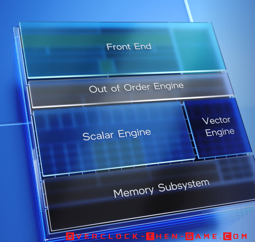
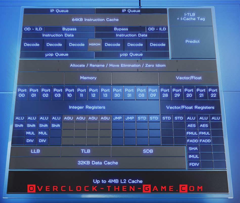
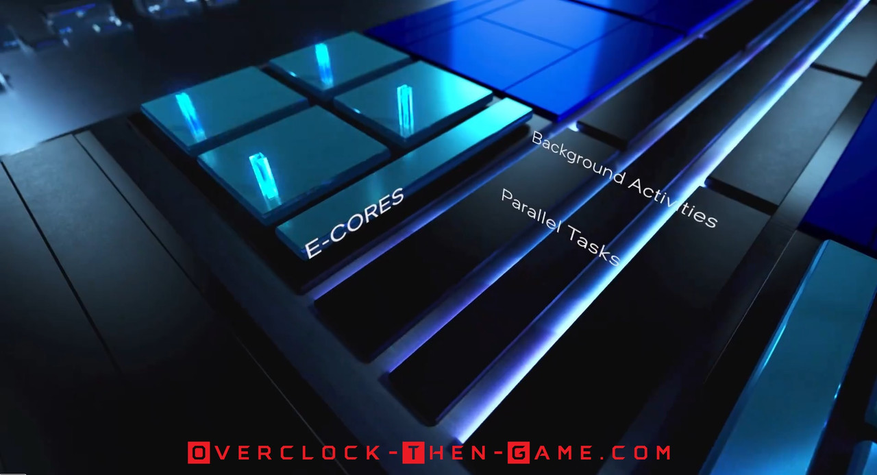
We will start with the Efficient Cores, codenamed Gracemont. Gracemont focus is throughput as it will be running the background tasks that don’t require a ton of performance to complete. The background tasks could be light workloads such as basic OS tasks or light workloads such as word processing software or web-browsing. As I stated previously these Efficient (E)-Cores do not include Hyper-Threading so they are limited to one thread per core. Intel did not want to add more complexity to an already monumental architecture and push Alder Lake out of the power budget that they have already set. Adding Hyper-Threading to the Efficient –Cores would have done just that, added more power and time to development. With future platforms I’m sure we could possibly see Hyper-Threading added to the efficient cores. Intel has deliberately decided to compare the Gracemont Cores to Skylake Cores (11th Gen) for Single-Theaded throughput performance. If the numbers hold true then the smaller Gracemont Cores could prove to be great for background tasks and efficiency. Intel has broken their Efficient x86 Core Microarchitecture into 5 areas, with those being: Front End (Instructions, Branch Prediction, and Decoding etc.), Out of Order Engine (scheduling, Allocation etc.), Scalar Engine (Execution Units), Vector Engine (EUs for complex data) and Memory Subsystem (L1 Data Cache, L2 Cache, TLB, SDB, LLB etc.). We will take a look at these different areas below in the architectural deep dive.
Gracemont vs Skylake
Intel claims that a 2-Core \ 4-Thread Skylake Core is slower than the 4-Core \ -4 Thread Gracemont (E)-Core with less power usage. This should be expected since Alder Lake E-Cores are being compared to the 11th Gen Skylake, however the bigger story is how much more efficient Gracemont is and how much more performance is gained with the 4C\4T (no Hyper-Threading) Gracemont Core over the 2C\4T (HT Enabled) Skylake Core. Intel is claiming an 80% performance increase while using 80% less in power usage in Multi-threading scenarios. That sounds like a great accomplishment if it holds true especially for Multi-Threading. Intel also says that the Single-Threaded performance when compared against Skylake (1C\1T) vs a 1C\1T (Gracemont) increases performance by 40% while decreasing power consumption by 40% which also sounds great.
Front End
Even without Hyper-Threading at the hardware level it appears that the Gracemont cores will perform well. We will now dive into the micro-architecture to see how this is possible. While trying to balance the power efficiency and performance ratio Intel decided on an Instruction Cache that has 64KB, which is double the Instruction Cache on my 1st Generation Nehalem\Westmere CPU (32KB Instruction Cache). Also unlike my 1st Generation CPU, the 12th Generation Gracemont Core apparently has the Instruction Length Decoder within the Instruction Cache. This will allow the decoder in later stages to have everything it needs while removing additional stages in the pipeline. On my 1st Generation Nehalem\Westmere CPU there were multiple stages with the Instruction Decoder and Queues. However, the Alder Lake-S L1 Data Cache remains the same as my 1st Gen CPU which is 32KBs. Intel is definitely making the Front End wider to keep the CPUs fed with plenty of data workloads. Gracemont can decode up to 6 instructions.
E-Core Memory Subsystem
I have been learning more about Intel memory subsystem and this is what I could gather. The L2 Cache can be 2MBs (Consumer Alder Lake-S) or up to 4MBs (Enterprise-Xeon) depending on the CPU model. That is an increase over Rocket Lake-S which had only 512KB and an increase over my 1st Gen CPU which contained only 256KBs. So in essence that is a 290% (2MB) to a 681% (4MB) increase in L2 cache memory over Rocket Lake and a 681% (2MB) to a 1,463% (4MB) over my 1st Gen Westmere CPU. Since Hyper-Threading is disabled on Gracemont Cores the larger L2 cache can help greatly within the cluster of cores and hopefully not waste long cycles on system memory reads. The L2 cache contains instructions and data unlike the L1 cache that splits the data and instructions. The 2MB L2 cache is shared between the 4 Gracemont cores (i7-12700K). If your CPU model has 8 Gracemont Cores (i9-12900K) then there are 2 clusters of Gracemont Cores. So the first set of cores in a cluster (x4 Gracemont Cores) will share the L2 memory cache and the second cluster (x4 Gracemont Cores) will share another L2 memory cache. That gives you a total of 4MBs L2 Cache if you have two Gracemont Clusters (i9-12900K\KF) which will be added to the Performance Cores total L2 cache discussed later in this article. Alder Lake supports up to 30MB L3 Cache I will speak more about the L3 memory later in the article in the “P-Core Memory Subsystem” section.
Instruction Cache Updates
So far this is pretty exciting. Intel says that Alder Lake will be there first “on-demand” Instruction Length Decoder that will be stored within the Instruction Cache. That should help with performance greatly since that step has been consolidated and will help the CPU decide if it needs to go through the entire decoder stage or not early in the pipeline. If the CPU recognizes the data\code then this process can be skipped, if the CPU does not recognize the data\code then the data can be processed quickly within the Instruction Cache. This way the CPU won’t have to necessarily wait for decoding that was traditionally in later stages like my older 1st Gen CPU. This wasn’t a big issue for many years, but consolidating workloads in the pipeline is always a great thing. To aid the workloads the branch target buffer has been increase to 5000 entries along with more history entries for branch predictions, this way the Gracemont Core can be as accurate as possible when working with instructions. Accuracy naturally leads to efficiency since Branch Predictions hits can lead to a better performance\power efficiency ratio without taking any other microarchitecture improvement into account. Deeper branch prediction cache means that misses can be caught and resolved before reaching crucial stages later in the pipeline which could cause stalls and hurt performance & efficiency.
Feeding the Beast & Power Efficiency
Moving down the Gracemont microarchitecture we see a much larger allocation buffer and out-of-order window. The clustered out-of-order decoder, as Intel calls it, can provide up to six instructions per cycle while holding a total of 256 entries (That is a 100% increase in entries over my 1st Gen CPU). This will feed the Execution Units via Ports and Gracemont comes packed with plenty of them for many operations per clock. Having such a large number of entries also allows more data to completed in parallel if there aren’t any dependencies. If all goes well the EU’s should always have plenty of data to execute. There are 17 execution ports for each Gracemont Core which should be capable of some serious parallel workloads. So if you have 8 Gracemont Cores (i9-2900K) then you theoretically could have 136 EU’s working at once if they are all being utilized for different purposes.
 If certain areas within the CPU aren’t being utilized Intel has included hardware that works alongside software that shuts down unused Cores, Execution Units and Ports within micro-seconds rather than milliseconds, according to Intel. However I have also read that this could get down to the nanoseconds. If Intel has been updating their old advance power-saving methods, and we know they have been, it is very possible that parts of the L2 cache will be in a very low power state if all regions of the L2 cache aren't being utilized after sometime. The same should be true for parts of the L3 cache as well.
There are 4 INT ALU, 2 FP\Vec as well as a Vector ALU. Intel packed 4 Total AGUs (x2 Store & x2 Load) which should help calculate addresses effectively for typical workloads. The Store\Load will be able to handle 32 byte reads. Intel has also included 2 FP\Vec Stores which should also be effective for complex related workloads. There are also 2 Jump ports and 2 dedicated Store Data EUs. Now we can begin to see how the Gracemont Cores are able to compete against Skylake Cores with potentially up to 80% more performance and 80% less power even though there is a lack of Hyper-Threading. Intel OOB scheduling must be top notch for this type of bold marketing. As far as I know the scheduler should able to send operations to any port as needed. All of this performance explains why Intel needed to increase the Instruction Cache, OOE entries and expanded on other areas within the core. The instruction sets for the Gracemont E-Cores use the same instructions that the Performance Cores (Golden Cove) uses. In order to use FP16 instructions the Performance Cores must be enabled. In order to use AVX-512 it appears that the Efficient Gracemont Cores will need to be disabled and the motherboard OEM will need to support or allow the feature.
So this tells me that even the Efficient Gracemont Cores alone should bring some big updates and performance increases to my archaic Intel X58 - 1st Gen 45nm (Quad) \32nm (Hexa) CPU build which only had a max of (32nm Westmere) 6 EU’s with 3 being dedicated for workloads (INT & FP\Complex) and 3 dedicated to memory operations (1 AGU (Load), 1 AGU (Store), 1 Store Data) per core. I am hoping that consumers can eventually have a streamlined approach to manually control which Cores applications can use (P-Core or E-Core).
If certain areas within the CPU aren’t being utilized Intel has included hardware that works alongside software that shuts down unused Cores, Execution Units and Ports within micro-seconds rather than milliseconds, according to Intel. However I have also read that this could get down to the nanoseconds. If Intel has been updating their old advance power-saving methods, and we know they have been, it is very possible that parts of the L2 cache will be in a very low power state if all regions of the L2 cache aren't being utilized after sometime. The same should be true for parts of the L3 cache as well.
There are 4 INT ALU, 2 FP\Vec as well as a Vector ALU. Intel packed 4 Total AGUs (x2 Store & x2 Load) which should help calculate addresses effectively for typical workloads. The Store\Load will be able to handle 32 byte reads. Intel has also included 2 FP\Vec Stores which should also be effective for complex related workloads. There are also 2 Jump ports and 2 dedicated Store Data EUs. Now we can begin to see how the Gracemont Cores are able to compete against Skylake Cores with potentially up to 80% more performance and 80% less power even though there is a lack of Hyper-Threading. Intel OOB scheduling must be top notch for this type of bold marketing. As far as I know the scheduler should able to send operations to any port as needed. All of this performance explains why Intel needed to increase the Instruction Cache, OOE entries and expanded on other areas within the core. The instruction sets for the Gracemont E-Cores use the same instructions that the Performance Cores (Golden Cove) uses. In order to use FP16 instructions the Performance Cores must be enabled. In order to use AVX-512 it appears that the Efficient Gracemont Cores will need to be disabled and the motherboard OEM will need to support or allow the feature.
So this tells me that even the Efficient Gracemont Cores alone should bring some big updates and performance increases to my archaic Intel X58 - 1st Gen 45nm (Quad) \32nm (Hexa) CPU build which only had a max of (32nm Westmere) 6 EU’s with 3 being dedicated for workloads (INT & FP\Complex) and 3 dedicated to memory operations (1 AGU (Load), 1 AGU (Store), 1 Store Data) per core. I am hoping that consumers can eventually have a streamlined approach to manually control which Cores applications can use (P-Core or E-Core).
Golden Cove – Architectural Deep Dive
Golden Cove = Performance Core
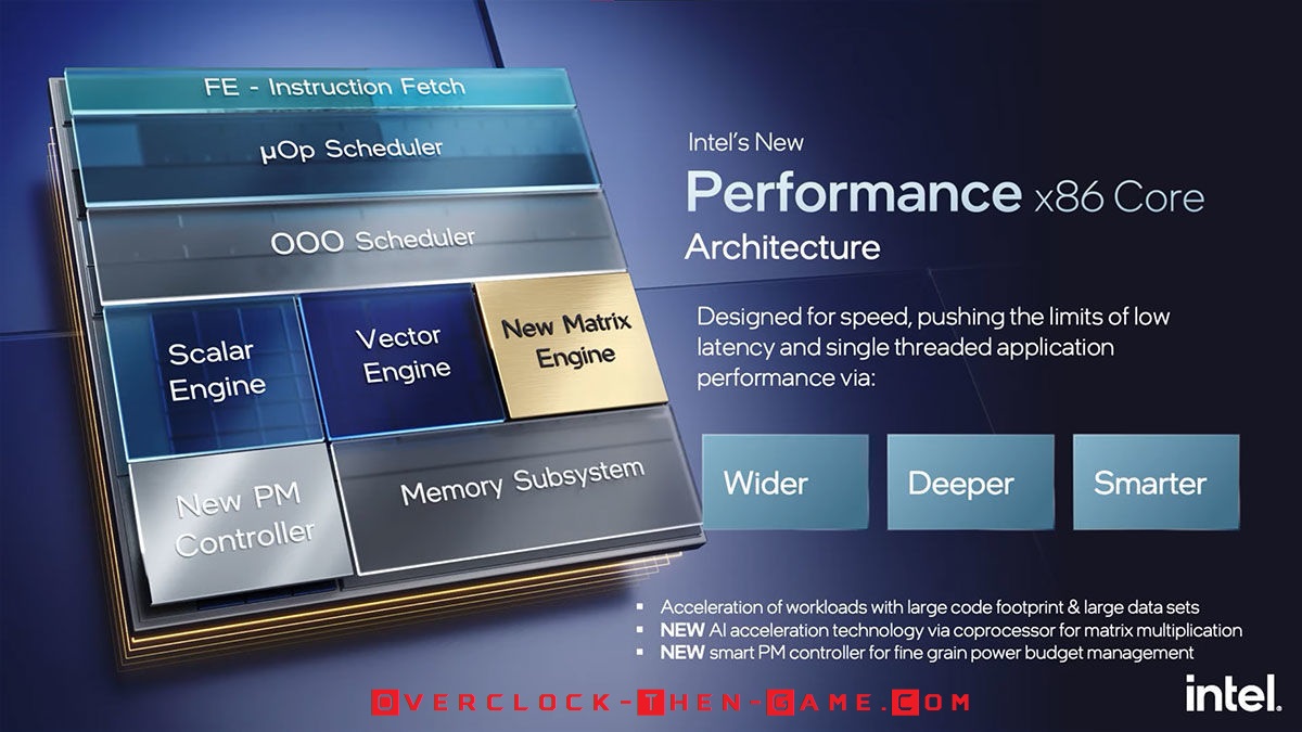
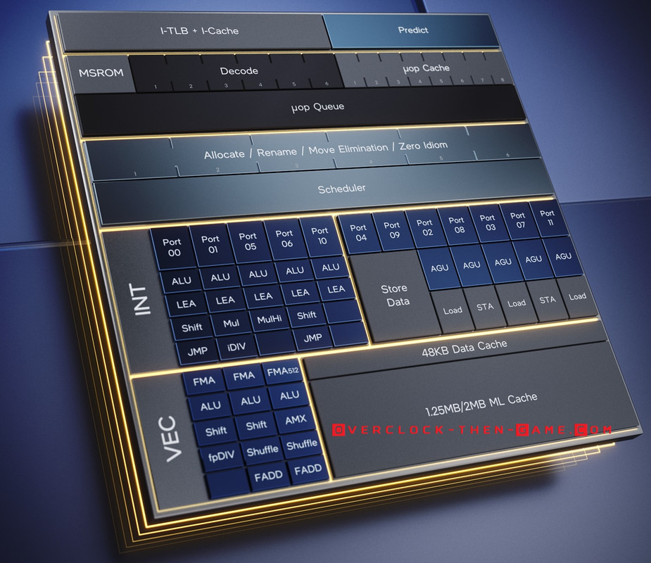
Now we move to the area that everyone will care more about, the Performance Core, codenamed “Golden Core”. Once again Intel is attempting to capture several markets with one design. The Performance Core goals are speed, single-threaded performance and low latency. As data and workloads are growing Intel designed the Performance Cores to be able to bring in more data and complete work on that data as effectively as possible. Although single-threaded performance is one of Intel's goals, the Golden Cove microarchitecture does support Hyper-Threading (SMT) unlike the Gracemont Cores. Golden Cove Performance x86 Core is broken down into areas, with those being: Instuction Fetch, uOP Scheduler, OOO Scheduler, Scalar Engine, Vector Engine, New Matrix Engine, New PM Controller, Memory Subsystem. So as we can see the Performance Core differs a bit from the Efficient Core.
Front End
Golden Core contains 32KB in L1 Instruction Cache, but the L1 Data Cache was increased to 48KB. The Length Decoder was increased to 32Bytes from 16Bytes found in the 11th Gen (Rocket Lake). As far as I am aware the Instruction Length Decoder is not in the Instruction Cache as found in the Gracemont Core. The branch target was increased as well to 12K branch targets which are up from 5K in the previous 11th Generation. Intel says that their branch predictor can hide many of the instruction cache misses, which could cause latency. Intel also claims that their branch predictor uses a machine learning algorithmic which can cause the branch predictor to grow or shrink its size and by size I believe Intel means its capacity\entries. Supposedly for programs that aren’t that large in size\code, the branch predictor can save power by turning off some of its area\capacity; however it can power up and expand its size when larger code is sent to the core. Intel seems to have set some ambitious goals with Alder Lake. Little things like this is what most people would look over, but it appears Intel is capable and feels comfortable talking about it.
Feeding the Beast
Intel has added two decoders that can output 6 micro-ops to the micro-ops cache (11th Gen could output 4). The uops cache can also hold 4K of data. The micro-ops cache can output 8 uops per cycle to the uops queue. From my understanding the uops queue can hold 72 entries per thread (SMT) and if it’s a single thread it can hold 144 entries. That is a 157% increase for SMT (Hyper-Threading) and a 414% increase for single-thread when compared to my 1st Generation CPU. The goal for Intel is to increase the hit rate to prevent long and wasted cycles that could mean transferring more data to and from the system memory. The out-of-order engine can allocate 6 uops and the reorder buffer can hold a staggering 512 entries which is also a 300% increase over my 1st Generation CPU. The goal in this case is to ensure that workloads can be scheduled accordingly, especially if there are no dependencies. Intel wasn’t joking when they said Alder Lake had a deeper out of order engine. To make all this work Intel uses their proprietary interconnect that allows the cores and core-memory subsystem to connect to the IMC.
Alder Lake Performance x86
Intel added an extra INT EU which pushes Alder Lake Execution Units to 5 for INT or none FP\Vector workloads. The extra EU contains the ALU and LEA only. The LEA is on all INT EUs and only takes 1 cycle for arithmetic calculations. LEA can also be used to quickly move information such as an address to a register and according to Intel, scaled operations all within a single cycle. Previously ADD operations were completed with the FMA units and took 4 cycles. For the Floating Points\Vector EUs Intel added two FADD (Fast Adders) on Ports 1 & 5. Intel claims that it only takes 3 cycles to complete in comparisons to FMA on the previous 11th Generation uarch (Rocket Lake) which took 4 to 6 cycles to complete depending on the port being used. Intel added an extra AGU Load EU pushing Alder Lake to 3 load ports (1 extra over the 11th Generation). There are a total of 12 Execution Units (up from 10 EUs on 11th Gen Rocket Lake) which means that if all of the Performance Cores are being utilized you can have up to 96 EUs being used at once across all 8 cores. If Intel has away for the Gracemont Efficient Cores to be used effectively with the Performance Cores for the same workloads then you could possibly have up to 232 EUs being used at once. In most cases they would be running different types of workloads, but Alder Lake is appearing to be a workhouse. The AVX-512 Instruction Set is supported with Alder Lake’s Performance Cores, but onlt if the Efficient Cores are disabled and the motherboard OEM supports\allows ASVX-512. AVX-512 will be available for the Enterprise\Server markets.

P-Core Memory Subsystem
Intel has decreased the latency even further when compared the 11th Gen Rocket Lake. Another difference between the Enterprise market and Consumer market is the L2 Cache size. Enterprise will get 2MB L2 Cache while the consumer market will only get 1.25MB Cache (my 1st Generation only has 256KB L2 Cache). That’s not too bad I suppose since the Enterprise markets will obviously need more performance and data throughput than the typical gamer sitting at home running synthetic benchmarks and games. Intel has tailored the L2 Cache to work in conjunction with the prefix engine and more than likely the branch prediction (front) engine so that the L2 Cache will hopefully know, by observing the data flowing into the cache, if more data instructions will need to be pulled from the system memory. This way the CPU won’t get stalled waiting for data if the L2 Cache can go ahead and fetch the data before it is needed. Alder Lake supports 9.5MB up to 14MBs L2 Cache. That is, 1.25MB for each Performance Core and 2MBs for each Efficient (Gracemont) Core. So for the i9-12900K \ KF (8 P-Cores + 8 E Cores) that would be 1.25MBs x 8 (P-Cores) = 10MBs L2 Cache for the Performance Cores. The Efficient Cores in two clusters (x4 Gracemont Cores) share 2MBs for a total of 4MBs L2 Cache. So that would be 2MBs x 2 (E Core Clusters) = 4MBs L2 Cache. Therefore the total L2 cache for the Core i9-12900 K \ KF would be (10MBs + 4MBs) 14MBs L2 Cache.
Alder Lake vs Rocket Lake
This comparison is much better than the 2015 Skylake comparison earlier with the Gracemont-Core. Intel is claiming that their 12th Generation “Alder Lake” Performance-Core is 19% faster than their previous 11th Generation “Rocket Lake”. This probably means that Alder Lake is trillions of times faster than my 1st Generation “Westemere”, especially the “Bloomfield” CPUs.
Alder Lake Features
Intel Thread Director
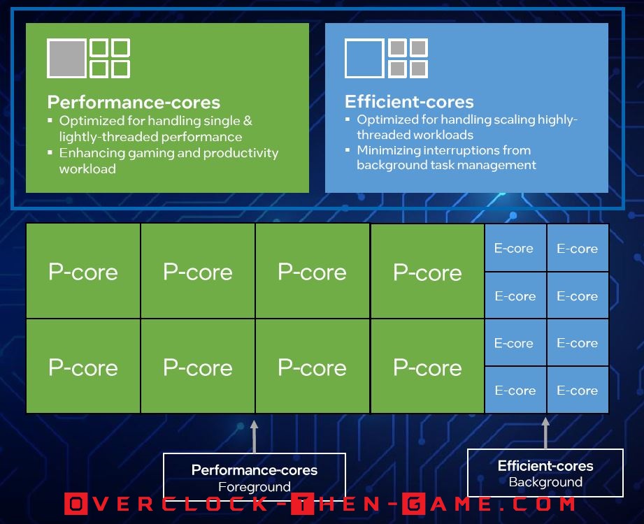
Now that we have learned about Alder Lake micro-architecture one has to wonder how the Performance-Cores & the Efficient-Cores complete workloads efficiently. That’s where the “Thread Director” comes into play. Intel, along with Microsoft, has created a solution between the software and hardware to determine which Performance or Efficient Cores will complete the workloads. This is accomplished by Intel’s Thread Director polling the instructions within the Core. To support this at the software level Windows 11 will be needed to take full advantage of this technology. Intel has been working closely with Microsoft to ensure that the Alder Lake microarchitecture can communicate with the Windows 11 OS effectively.
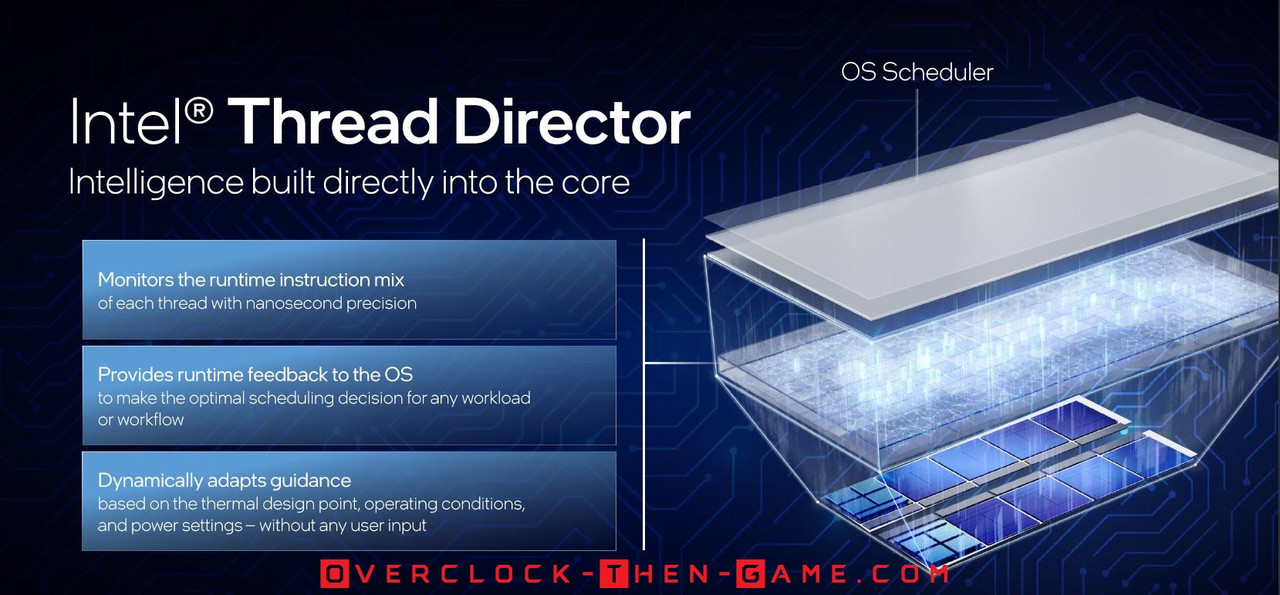
In real-time Alder Lake sends feedback to the Windows 11 OS to ensure that the OS task scheduling is sending data to the cores that can complete the workloads efficiently. Each core will be reported to the OS down to the nanosecond to ensure that workloads are sent to specific cores based on several criteria’s. Normally background tasks will be sent to the Efficient-Cores and priority tasks will be sent to the Performance-Cores. As an example, if you are playing a video game then the game threads will be sent to the Performance-Cores, while the Windows 11 OS background tasks and streaming software threads will be sent to the Efficient-Cores. It appears that Intel’s Thread Director at the hardware level will be even smarter than we think since it will be able to move tasks from the Performance-Cores over to the Efficient-Cores when needed in real-time. If you were working with multiple software and needed to multitask this could be a great thing. Alder Lake should make multi-tasking quicker. Let’s say you were working in Blender on a scene, but you realized that you needed to make some last minute changes to an object in Zbrush. Well initially Blender would be the main window that you are using (“Foreground” App :: Performance Cores) and when you switch over to Zbrush, Intel’s “Thread Director” would move Blender threads to the “background” (Efficient Cores). Now that you currently are working Zbrush and it is the Foreground App it will run on the Performance Cores. Let’s say you decide to export the model in Zbrush and switch back to Blender. Blender would now be the Foreground App and the Blender threads would switch from the Efficient Cores to the Performance Cores while Zbrush threads would switch to the background Efficient Cores during exporting. Supposedly this type example will be a seamless transition between the P-Cores and E-Cores. When it comes to video game engines things might not be as simple as it is with typical Windows OS scheduling. Certain gaming tasks need to ran on the Performance-Cores for the best results while other less important tasks should be ran on the Efficient-Cores. Traditionally developers could just locate how many processors (physical & logical cores) were on a PC and issue threads to those CPU cores. That is no longer the case and Intel recommends that video game developers differentiate between the Performance-Cores and Efficient-Cores for maximum performance. Intel will still allow the “Intel Thread Director” to be used, but it is recommended that developers optimize the game engine for scheduling. Intel is working to allow more usage with Alder Lake P & E-cores by allowing the usage of the “Power Throttling” API which will allow developers to determine which threads are more important than others. This can greatly help the Thread Director. Even if developers do not use the Power Throttling API the Windows 11 OS scheduler (software) and Intel’s Thread Director, from a hardware standpoint, can still ensure current and future software can run efficiently across the Alder Lake P & E-Cores without any intervention from the developers. If Intel and Microsoft can pull this off this will be a game changer for sure. It is worth noting that Windows 10 does support Intel’s Thread Director, however it is an older version which does not allow the Alder Lake architecture to provide feedback to the OS. This means that threads won’t be scheduled to the correct cores in real-time.
Alder Lake Memory Technologies
DDR4 - DDR5
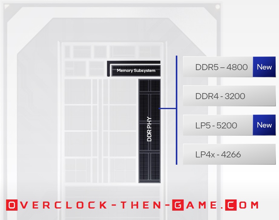 Intel is once again leading the charge by bringing new technology to the public and will be the first to bring DDR5 to the market. Not only will Intel be supporting DDR5 (4800Mhz), but Alder Lake will also be supporting LP5 (Low-Power DDR5 (5200Mhz)), DDR4 (3200Mhz) and LP4 (Low-Power DDR4 (4266Mhz)). So enthusiast will have the choice between the current DDR4 DRAM Modules or the latest and greatest DDR5 DRAM modules. The Low-Power DDR 4 & 5 modules will more than likely be aimed at mobile users and other small devices (SODIMM). That’s not to say that LPDDR4\5 won’t be available for desktop users. Normally the Low-Power DDRx Modules are for the Enterprise\Server or Mobile markets. Intel will also support overclocking the modules in many ways (software and hardware).
Based on early reviews we noticed that Alder Lake has higher latencies when using DDR5, but more throughput and bandwidth. The opposite was true for DDR4 which had lower latencies, but also less throughput and bandwidth. As DDR5 matures we expect this to change in the near future. So there will be a balance that needs to be met, but it’s great to have more than one option. Alder Lake will support power management features that will allow the CPU to disabled specific areas in the memory subsystem and\or the Integrated Memory Controller (IMC) in order to save power and prevent interference.
As the CPU enter lower power states (C-states) these features will be enabled. From my understanding if you do not occupy all of the DRAM memory slots on the motherboard the Alder Lake CPU will disable specific areas of the Memory Subsystem\IMC, as I stated earlier, to save power and prevent possible interference between the signals. The IMC is used to transfer data from the system DRAM to the Alder Lake CPU. Since Intel is supporting both DDR4\LP4x and DDR5\LP5x, Alder Lake implements two different memory controllers and both supports dual channels. They cannot be used interchangeably. I suppose that it is possible to mix DDR4 and DDR5 on a motherboard, but the IMC will only see half of the total memory on the motherboard. However, Intel only allows one type of DDR type on a system so mismatching DDR4 & DDR5 won’t be allowed. You will have to choose between DDR4 or DDR5 when choosing a motherboard.
In addition to Alder Lake memory controller being able to lower (or higher) the power usage and capacity, it will be able to determine this scaling based on various criteria’s. Some criteria’s could be time-critical workloads that require low latency while other workloads might require high bandwidth, but for workloads that are neither time-critical and doesn’t require a lot of bandwidth the IMC can run at low power-low frequency (Gear-4). Most enthusiasts are familiar to the term “Gears” that Alder Lake’s IMC can use. Alder Lake has several Gears that will correspond to real-time workloads and various scenarios. These Gears are based on the mathematical ratio between the memory controller frequency and the DRAM frequency with the number following the term “Gear” being the IMC ratio (‘1:2’ ratio = “Gear-2”).
The goal for most enthusiasts, overclockers and gamers will typically be Gear 1 (1:1 ratio) which allows the IMC to run at the same speed as the DRAM. Or course this causes the CPU to use more power, but allows the lowest latency and highest bandwidth usage between the IMC and the DRAM. Alder Lake’s IMC is rated to run at (DDR4) 3200Mhz & (DDR5) 4800Mhz. With default settings DDR4 will run at Gear 1 and DDR5 will run at Gear 2. With DDR5 already hitting some pretty high frequencies such as DDR5-6800Mhz as a standard, there is no telling how far we will be able to push Alder Lakes memory controller frequency to match the DDR5 frequency. It’s safe to say that enthusiast\overclockers will be trying their best to use the lowest Gears possible (Gear 1 = 1:1) with high DRAM overclocks.
Intel is once again leading the charge by bringing new technology to the public and will be the first to bring DDR5 to the market. Not only will Intel be supporting DDR5 (4800Mhz), but Alder Lake will also be supporting LP5 (Low-Power DDR5 (5200Mhz)), DDR4 (3200Mhz) and LP4 (Low-Power DDR4 (4266Mhz)). So enthusiast will have the choice between the current DDR4 DRAM Modules or the latest and greatest DDR5 DRAM modules. The Low-Power DDR 4 & 5 modules will more than likely be aimed at mobile users and other small devices (SODIMM). That’s not to say that LPDDR4\5 won’t be available for desktop users. Normally the Low-Power DDRx Modules are for the Enterprise\Server or Mobile markets. Intel will also support overclocking the modules in many ways (software and hardware).
Based on early reviews we noticed that Alder Lake has higher latencies when using DDR5, but more throughput and bandwidth. The opposite was true for DDR4 which had lower latencies, but also less throughput and bandwidth. As DDR5 matures we expect this to change in the near future. So there will be a balance that needs to be met, but it’s great to have more than one option. Alder Lake will support power management features that will allow the CPU to disabled specific areas in the memory subsystem and\or the Integrated Memory Controller (IMC) in order to save power and prevent interference.
As the CPU enter lower power states (C-states) these features will be enabled. From my understanding if you do not occupy all of the DRAM memory slots on the motherboard the Alder Lake CPU will disable specific areas of the Memory Subsystem\IMC, as I stated earlier, to save power and prevent possible interference between the signals. The IMC is used to transfer data from the system DRAM to the Alder Lake CPU. Since Intel is supporting both DDR4\LP4x and DDR5\LP5x, Alder Lake implements two different memory controllers and both supports dual channels. They cannot be used interchangeably. I suppose that it is possible to mix DDR4 and DDR5 on a motherboard, but the IMC will only see half of the total memory on the motherboard. However, Intel only allows one type of DDR type on a system so mismatching DDR4 & DDR5 won’t be allowed. You will have to choose between DDR4 or DDR5 when choosing a motherboard.
In addition to Alder Lake memory controller being able to lower (or higher) the power usage and capacity, it will be able to determine this scaling based on various criteria’s. Some criteria’s could be time-critical workloads that require low latency while other workloads might require high bandwidth, but for workloads that are neither time-critical and doesn’t require a lot of bandwidth the IMC can run at low power-low frequency (Gear-4). Most enthusiasts are familiar to the term “Gears” that Alder Lake’s IMC can use. Alder Lake has several Gears that will correspond to real-time workloads and various scenarios. These Gears are based on the mathematical ratio between the memory controller frequency and the DRAM frequency with the number following the term “Gear” being the IMC ratio (‘1:2’ ratio = “Gear-2”).
The goal for most enthusiasts, overclockers and gamers will typically be Gear 1 (1:1 ratio) which allows the IMC to run at the same speed as the DRAM. Or course this causes the CPU to use more power, but allows the lowest latency and highest bandwidth usage between the IMC and the DRAM. Alder Lake’s IMC is rated to run at (DDR4) 3200Mhz & (DDR5) 4800Mhz. With default settings DDR4 will run at Gear 1 and DDR5 will run at Gear 2. With DDR5 already hitting some pretty high frequencies such as DDR5-6800Mhz as a standard, there is no telling how far we will be able to push Alder Lakes memory controller frequency to match the DDR5 frequency. It’s safe to say that enthusiast\overclockers will be trying their best to use the lowest Gears possible (Gear 1 = 1:1) with high DRAM overclocks.
PCIe Technologies
PCIe 5.0 x16
Intel is the first company to release PCIe 5.0 to the consumer market with Alder Lake. Alder Lake will support a direct connection to a single PCIe 5.0 (x16 mode) slot or dual PCIe 5.0 (x8 mode). PCIe 4.0 (x4 mode) will be directly connected to the CPU as well for a SSD or Intel “Optane” Memory\Storage. Regardless of how many PCIe slots the motherboard manufactures add (x1 or x2 PCIe 5.0 slots) the CPU will support a single PCIe 4.0 running x4 mode (8GB\s). PCIe 5.0 (x16) can theoretically use up to 64GB\s with ease. PCIe is backwards compatible so any PCIe device or SSD (M.2 in this case) should work with no problems. The Z690 chipset will be capable of running PCIe 4.0 (x12) and PCIe 3.0 (x16), but I will speak more about the Z690 Chipset on the next page. For users, such as myself, who can easily run a desktop for well over half a decade there is plenty of upgrade potential if needed. The main reason that Intel decided to use PCIe 4.0 (x4 mode) was due to the increased processor die size and logic requirements. It was easier to follow the already established 20 lanes on the 11th Gen. PCIe 5.0 (x4) would have taken up more space and PCIe 5.0 (x16) was already much larger than PCIe 4.0 [I/O] on the 11th Gen CPUs. Using PCIe 4.0 will allow more flexibility when using more PCIe 4.0 lanes (1x4 mode, 2x8 mode etc.)
Alder Lake's Blazing Speed & Power Usage
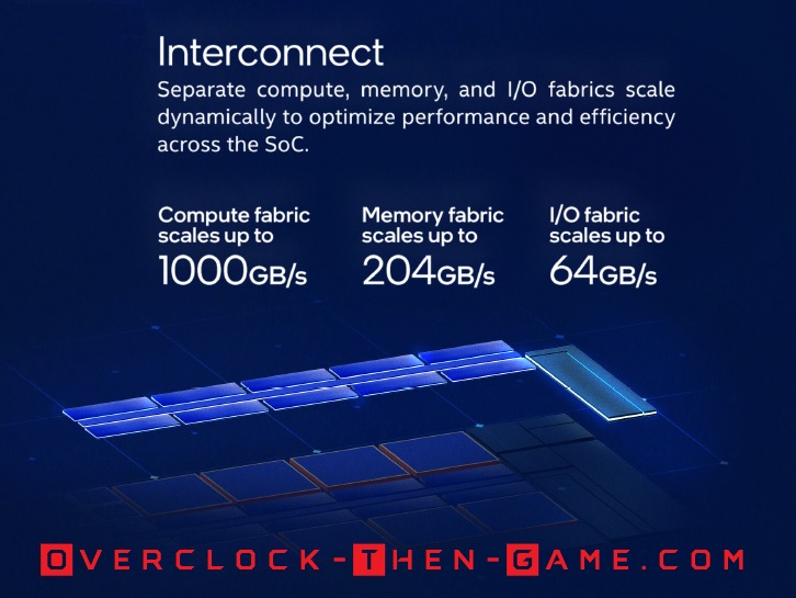
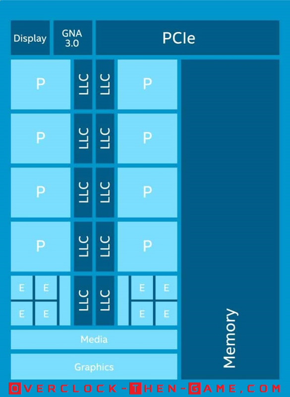
Intel’s Alder Lake is capable of some impressive speeds within the CPU micro-architecture. Intel created three separate interconnect fabrics to ensure that the micro-architecture is scalable. This means that Alder Lake bandwidth and performance should not be compromised across multiple market segments when scaled. These interconnects are also able to report various information such as current loads on the fabric which will allow data to be directed to the most effective Core for completion. This is also true for the I\O and memory subsystem which can scale their speeds and\or bus width which can lead to low-latency scenarios, more performance if needed or power saving features. Intel states that Alder Lake can get up to 1000 GB\s or 1TB in dynamic latency optimization between the Cores (P & E cores) via the fabric used to connect them together. That would be 100GB\s for each Golden Cove Performance-Core and for each cluster Gracemont Cluster Core (x4 E-Cores). Intel's Alder Lake CPU I\O interconnects can get up to 64GB\s in real time which should be expected since PCIe 5.0 (x16) is the standard for Alder Lake I\O. However, one must wonder if Intel made a mistake since the CPU I\O can support up to 3 devices if utilized which means the total bandwidth should be around 71.8GB\s. If the I\O interconnects follow the PCIe specifications then the Alder Lake CPU should comply and actually use nearly 72GB\s if needed. Otherwise there could be bottlenecks, but I honestly do not believe that the PCIe 5.0 slot(s) will be used to its full potential (64GB\s). As far as Alder Lake Memory Subsystem goes Intel claims up to 204GB\s of bandwidth. That seems to be very impressive. I’m sure there will be synthetic benchmarks available to give more insight into these claims. Alder Lake will also support hardware acceleration for Microsoft's Direct X 12 pipeline. Intel has decided to use the same Xe-LP integrated graphics uarch that was used in the 11th Gen, however we should see some improvements due to architectural changes. Alder Lake supports Intel’s Turbo Boost Max Technology 3.0. This version allows cores to individually change their core frequency. The Operating System will need to support dynamic per-core frequencies and can be used to assign workloads to cores based on several criteria’s for low power and high performance scenarios.
Intel's Z690 Chipset
Now that we have learned about Alder Lake’s microarchitecture and features we will switch the focus to the Z690 chipset. To support the high-speed coming to and from the CPU Intel has upgraded several key areas. To ensure that all of the new and fast technology has the required bandwidth Intel has updated their DMI 3.0 to DMI 4.0. DMI 4.0 is two times faster than DMI 3.0. Intel’s DMI 4.0 is the link between the Alder Lake CPU and the Z690 chipset and supports up to 8GB\s (bi-directional) so that comes out to 16GB\s. For comparison my 1st Generation X58 chipset used DMI 1.0 (QPI) which topped out at a blazing 2GB\s (bi-directional – 4GB\s) which makes DMI 4.0 four times faster than my X58 DMI\QPI link.
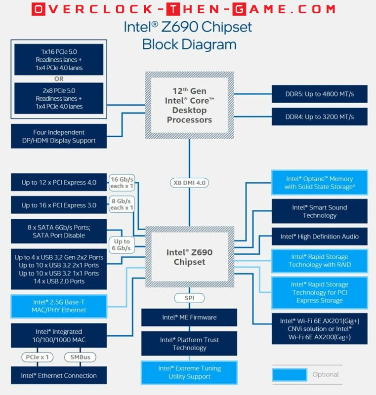
The Z690 Chipset supports PCIe 4.0 and 3.0. Intel states that the Z690 supports up to sixteen PCIe 4.0 connections running at x1 speeds (16 Gb\s) and up to 12 lanes. Motherboard manufactures will be combining these lanes and so far it appears that PCIe 4.0 running x8 mode (64 Gb\s) will be the standard for most PCIe connections. Many of the PCIe 4.0 lanes will more than likely mostly be used for M.2 SSD storage and other on-board features listed below. PCIe 3.0 will use up to 16 lanes. There are a ton of motherboards releasing with the Z690 chipset so there is no telling how many variations will be released over the next year or so. Intel’s Z690 Chipset is 14nm for those who might be wondering.
USB 3.2 (5Gb\s) and USB 3.2 (10Gb\s) are supported as well. Each USB 3.2 Gen ports (5Gb\s & 10Gb\s) will support up to 10 devices. USB 3.1 Gen 2 (20Gb\s) will support up to 4 devices. Although USB 3.x is backwards compatible USB 2.0 hasn’t gone anywhere. Intel will continue to support up to 14 USB 2.0 ports. Ethernet speeds of 1 Gbps will still be the standard, but the Z690 Chipset will natively support 2.5Gbps if the motherboard OEMs decide to support it as an option. 2.5Gbps will be overkill for most home users. Intel’s Optane Memory\Storage will be supported on the chipset as well. As far as RAID goes all of the standard RAID configurations (0, 1, 5, 10) will be allowed for both SATA and PCIe. Intel will allow native and discrete support for their Wi-Fi 6E. Intel’s Z690 chipset will allow OEMs to change many of the high-speed lanes. This is supported due to many different types of technology standards that the manufactures can specify as they see fit. Certain lanes won’t be changeable such as the DMI lanes or other reserved lanes, but other lanes, for instance PCIe 3.0 & 4.0, can be used for various purposes such as Gigabit Ethernet or 2.5Gb Ethernet, M.2 slots, SATA ports and so on. So for PCIe there is a maximum of 28 PCIe lanes, but only 12 PCIe 4.0 lanes are usable due to the other remaining 16 lanes being reserved for PCIe 3.0. For example a motherboard that I was viewing supports three PCIe 4.0 “M.2” slots in “x4 mode” which comes out to 12 lanes. This would leave that motherboard OEM left with 16 PCIe 3.0 lanes for various I\O ports (USB, Ethernet etc.) Obviously this will allow OEMs to create many tiers and SKUs for the Z690; all with different features and options.
12th Generation Overclocking
The last platform I have overclocked was the 2008 X58 platform that Intel released more than 13 years ago. There were many options and settings to tweak. It was a great and fun experience during that era. After the X58 platform overclocking on newer platforms started to be mostly reliant on overclocking the Voltage and CPU Ratio’s with various settings such as the Base Clock (BCLK) & PCIe Frequency being locked. I also understand why Intel decided to lock down certain frequencies as well, but the enthusiast platform has always been “High Risk – High Rewards”. Alder Lake and the Z690 Chipset have made me excited about overclocking again.
Specifications
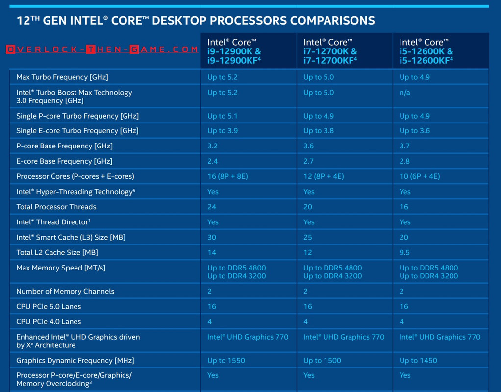
Now we will take a look at some of the hardware that I decided to purchase. I tried to maximize my performance and get what was available. The Intel Core i9-12900K packaging was very nice and clever for the higher-end models. You can really tell that they put a lot of thought into their 12th-Gen package. The higher end i9-12900K & KF does not come with a packed in stock cooler, but some of the lower models do include the cooler. I decided on using stock DDR5 RAM Frequency (4800Mhz) to show the default performance. I am very interested in learning more about the Alder Lake micro-architecture and attempting to replicate some of Intel claims. I decided to go with the “ASUS ROG Strix Z690-F Gaming Wi-Fi”. ASUS allows me to use a LGA1200 cooler on the Alder Lake LGA1700 socket. So later we will see how well the the LGA1200 360mm Rad AIO cools the i9-12900K.

CPU: Intel Core i9-12900K
CPU Cooler: EK AIO 360mm Liquid Cooler
Motherboard: ASUS ROG Strix Z690-F Gaming Wi-Fi
RAM: 32GB DDR5-4800Mhz [2x16GB]
PSU: Phanteks 1200W - 80+ Platinum
SSD: 1TB WD BLACK SN850 - 7.0GB\s Read - 5.3GB\s Write - PCIe Gen4 (x4)
SSD: 3TB - 2.7GB\s Read - 2.1GB\s Write
HDD: 6TB - 350MB Read - 330MB\s Write - RAID 0
GPU: EVGA RTX 3080 Ultra Liquid Cooled 240mm - Push
GPU Speed: 1440Mhz
(Stock) –
Core: Mhz (Mhz Boost) - 1845Mhz
GPU vRAM: 10GB
GPU Drivers: Geforce: v496.76 [Nov 16, 2021]
Alder Lake Core Latency

Now that I have had a few days to play around with my i9-12700K we can take a deeper dive into the microarchitecture. Since this is a completely different micro-architecture than previous Intel releases I have tried to gain as much accurate information as I could. Some of this information I present below could change as I continue to learn more about Intel’s Hybrid Technology. Latency plays a big part in performance and there’s a balance that must be met in regard to bandwidth. Let’s take a look at Alder Lake’s core latency.
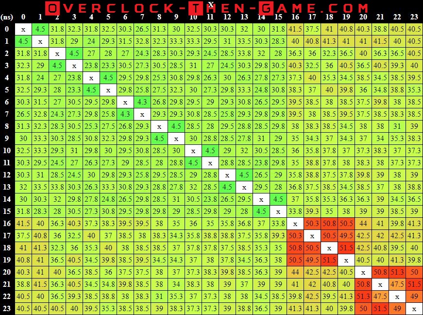
Performance Core Latency
P-Core to P-Core Latency Average = 27.59 ns P-Core to P-Core Latency Minimum = 4.25 ns P-Core to P-Core Latency Maximum = 33.75 ns
Starting with the Performance Core (#0 to #15) latency we see that the average is 27.59ns. The lowest latency recorded was 4.25ns (rounded to 4.3) on Core #7. The highest latency recorded was 33.75ns (rounded to 33.8) between Core #2 and Core #13. Overall this isn’t that bad at all, well that is until the P-Core needs to communicate with the E-Core. At that point the latency begins to climb for certain P-Cores. As expected the further the P-Cores are away from the E-Cores the more latency is gained. For example, Performance Core #3 has 40.3ns latency to Efficient Core #16. However, the Performance Core #15 only has 33.8ns latency to Efficient Core #16.
Efficient Core Latency
E-Core to E-Core Latency Average = 40.2 ns E-Core to E-Core Latency Minimum = 31.0 ns E-Core to E-Core Latency Maximum = 51.5 ns
Moving down to the Efficient Cores shows much higher Latencies. The Efficient Cores are smaller Intel Atom Cores that are clustered together in groups of 4. The i9-12900K has two clusters with each cluster containing 4 Efficient Atom Cores (2 Clusters x 4 Atom cores = 8 Cores). Cores #16 to #23 are our Atom cores. The average latency amongst the E-Cores is 40.2ns with the lowest latency recoded showing 31ns. Since the 8 Atom Cores are grouped into a cluster of 4, the maximum latency is very high. Earlier in the article (Gracemont Core – Architectural Deep Dive) I explained how each cluster (4 E-Cores) shares a single L2 cache. This can cause high latency when compared to the P-Cores. This benchmark also shows us how the Atom Cores are paired within the architecture. For data to travel from one cluster to the next means that it must travel across the shared L2 Cache and the L3 Cache (LLC), unlike the Performance Cores which doesn’t need to share the L2 Cache with other Cores.
Individual Core & Cache Latency
Prior to Alder Lakes release I was fascinated with Intel’s Hybrid Technology and their new take on the well-known big.LITTLE architecture. I had many questions and I had to find the answers to my questions. Perhaps my interest will answer questions for others who may have had the same thoughts. Now we are going to dive a little deeper into the micro-architecture and take a look at other latencies within Alder Lake-S. It is extremely hard to benchmark cache performance and normally I would just run various well know memory benchmark tools, but Intel’s Hybrid Technology is so new that some of the popular tools cannot properly benchmarks on the Alder Lake uarch. Therefore I will try my best to determine how well Alder Lakes micro-architecture performs. Let’s take a look at Alder Lake-S latency to system memory (DRAM).
Alder Lake-S CPU Latency to System Memory (DRAM – DDR5-4800Mhz CAS40) = 75.4 ns
Alder Lake-S CPU Latency to System Memory (DRAM – DDR5-4800Mhz CAS40) = 75.4 ns
Prior to the Alder Lake release we knew that DDR5 would bring higher latencies and much higher CAS therefore high latency was expected. Due to how Intel developed Alder Lake the latency numbers will differ slightly. The cores can quickly enter and leave C-states\low-power states which can affect the latency. During my benchmarks I noticed that the Cores would be in certain C-states since the Intel Thread Director & Windows Scheduling doesn’t always consider every workload a major task. All of the test presented shows my PC running stock settings. Now we will check out the latencies for each individual core to the system memory (DRAM).
Alder Lake Individual Cores Latency To DRAM
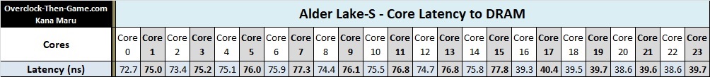
We see that the P-Cores (Core0 to Core15) have much higher latency when compared to the E-cores (Core16-Core23). I thought this was very interesting. The Efficient Cores can access data to and from DRAM by as much as 1.9 times faster than the Performance Cores. It should be noted that this benchmark tests random memory locations as well. The Performance Cores latency is 92% higher than the Efficient Cores. Now we see how the Efficient Atom Cores obtain efficiency and high throughput. It also helps that the Efficient Cores are Single-Threaded (no Hyper-Threading\SMT). Now let’s move down the memory hierarchy and check out the lower layers.
Alder Lake Individual Cores Latency To L3 Cache
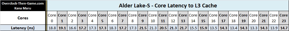
I have updated my chart above to reflect my latest benchmarks. While still using random memory locations, we can see various changes in latencies for each core. We must remember that each core frequency can be individually different from one another; this was introduced with Intel’s Max Turbo3.0. Therefore we can see different results for each core. For example, while the average latency for all Cores was 17ns, the lowest latency recorded was 13.3ns and the highest latency is 21.7ns. I purposely wanted to use these results to show how much of a difference we can expect when leaving idle periods and sending workloads to the cores. Despite the high latency on one core (#13) on average the P-Cores latency is 18.55ns while the E-Cores average 13.96ns.
Alder Lake Individual Cores Latency To L2 Cache

The P-cores show 2.0ns – 2.1ns. As I go deeper into the uarch it becomes harder to benchmark the E-cores, but we can see that they all share a similar latency (5.2ns). This could be due to the fact that they are clustered and share the same L2 cache. As a reminder there are two L2 Caches for the Efficient Atom Cores and each L2 cache contains 4 Atom Cores.
Alder Lake Individual Cores Latency To L1 Cache
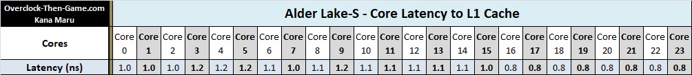
Now that we are directly on the core we can take a look at how low the L1 cache latency can get. Latency to the P-cores show approx. 1.1ns and all of the Efficient Cores show the same latency at 0.8ns. It is possible that these numbers will vary, but these numbers appear to be fairly accurate. In this benchmark the Efficient Cores appear to outperform the Performance cores by 20%.
Alder Lake Individual Cores Latency To All Levels
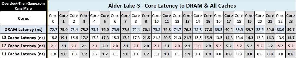
Here is a picture wrapping up my benchmark results. Here we can see all of the different levels and latency for the Alder Lake micro-architecture. The Efficient Core results were surprising in relation to the system memory (DRAM) since I expected those E- Cores to have much higher latency or at least have latency near the Performance Cores. Instead the Efficient Cores appear to be, well, efficient. I haven’t even begun to overlock the platform yet and I can’t wait to see what I can accomplish as I continue to learn about the Alder Lake uarch.
Alder Lake Interconnect Bandwidth
If you can recall earlier in the article I spoke about how Intel claimed that Alder Lake-S would support up to 1000 GB\s or 1TBs of bandwidth within the microarchitecture. Well I wanted to know how much bandwidth I could get with my Alder Lake-S CPU and DDR5-4800Mhz running default settings. DDR5-4800Mhz is the official supported DDR RAM frequency, but of course Alder Lake is capable of handling much higher DRAM frequencies. I ran a lot of low-level benchmarks on Alder Lake in relation to the DDR5-4800MT\s and I was surprised from what I learned. However, the architecture is brand new and I am seeing all types of performance numbers. Some of the software I use doesn’t know what to do with the CPU and I am trying to look past all of the bad data since its already hard enough to benchmark a micro-architecture as it is. The results below will use various workload scenarios to determine the ending results. With all of that being said we will take a look at all cores (P & E Cores) and see how much performance I can get when all 16 Cores & 24 Threads work together.
Performance & Efficient Cores
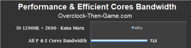
I was able to pull 713GB\s of total bandwidth in my test. That’s fairly close to 1000 GB\s, but we must remember that the 1000GB\s (1 TB\s) bandwidth that Intel claimed isn’t all dedicated to the cores so I consider this a fair number. Another thing to consider and one you might want to refer back to is the latency chart on the previous page. Latency plays a big part in bandwidth performance and the result above is an aggregate of different workloads. If you recall the E-cores can have massive spikes in latency and the further the cores are away from each doesn’t help matters either.
Performance Cores Bandwidth (8 P-Cores)
Now that we have seen how well the P & E Cores work together let’s see how well they work separately. We will start with the Performance Cores and see how much Bandwidth I can achieve with them working together without the Efficient Cores.
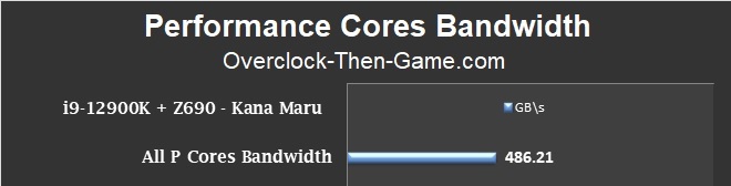
The Performance Cores were able to pull 486 GB\s on average. However, I recorded the top bandwidth performance maxing at an incredible 1.72 TB\s (Terabytes)! Obviously the 1.72 TB\s and 1.35 TB\s I recorded would be under the absolute best scenario which is why I prefer to use many different workloads to aggregate the typical performance. We will visit the best case scenarios and maximum performance for Alder Lake P and E Cores later in this article. One thing I noticed is that the Intel Thread Director and Intel’s Turbo Max is very aggressive with the low-power modes. Although I explained this earlier in the article I would like to repeat that the Alder Lake-S CPU runs DDR5 in “Gear 2” by default (DDR4 = Gear 1). So that means my LLC clock is only at 3600Mhz for the majority of all benchmarks thus far according to my monitoring software. Occasionally it would jump to 4700Mhz, but quickly drop back down to 3600Mhz. So it is possible that I will be able to gain more performance as I begin to overclock the CPU.
Efficient Cores Bandwidth (8 E-Cores)
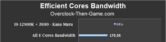
In this benchmark I attempted to determine how much performance I could get from both clusters containing only the Efficient Cores (x2 Clusters = 8 E-Cores). Although the Efficient Cores individually are capable of some serious bandwidth performance, as we will see shortly in this article, the latency amongst the E-Cores clusters shown earlier should be taken into consideration as that will affect bandwidth. However, with each individual E-Core they have quick access to the L2 Cache, L3 Cache and DRAM based on my testing. The best performance BW I recorded was 413.43 GB\s. The average was 176GB\s so it’s safe to say that the E-Cores are well equipped to handle various workloads.
One Efficient Cluster Bandwidth (4 E-Cores)
In the previous benchmark we saw both Efficient Clusters (8-cores) working together. Now I would like to take a look at how well each Cluster works independently (4-Cores). This should show the “best case” scenario since only 4 Efficient Cores will work on the same workload and not have to worry about the long cycles and\or latency to the second Efficient Cluster (or the Performance Cores).
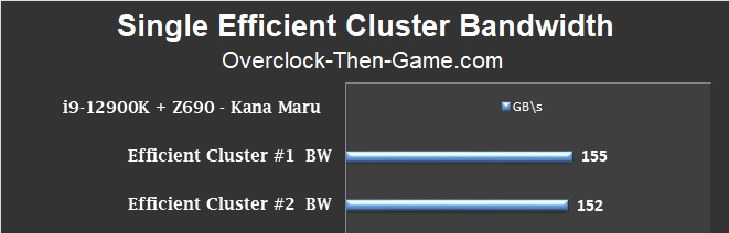
This benchmark shows how efficient both Clusters can be if they are working on separate workloads. As long as the Efficient Clusters doesn’t need to share data between each other, or limited sharing, we see that it is possible to accomplish roughly 307 GB\s. That would make the Efficient Clusters (at 307GB\s) about 54% slower than the Performance Cores. When the Efficient Cores were working on the same workloads we saw the performance drop to only 176GB\s earlier, but each Cluster performed very well when separated. This could simply be a software limitation to the new Intel Hybrid Architecture. I will continue to monitor this behavior, but I thought I would share my results. If Intel and Microsoft can ensure that specific workloads can stay within a certain cluster then they would avoid the high latency issue which affects bandwidth. This would allow the separate Efficient Clusters and the Performance Cores to theoretically output around 782 GB\s when working on separate workload threads. This would make the Efficient Cores extremely efficient even at stock settings. In the absolute best case scenario the bandwidth max was 389 GB\s on Efficient Cluster #1 and 387 GB\s for Efficient Cluster #2.
All Performance and Efficient Core Results
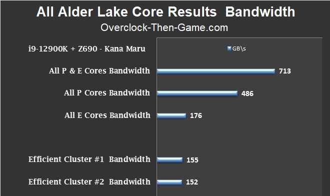
This chart will give a clearer picture to the differences between the P & E Cores. We can see the difference between the core segments (P and E) and how well they work together. So although I did hit 713 GB\s with all cores working together as I stated earlier Intel didn’t state that the total 1000 GB\s interconnect speed wasn’t solely dedicated to only the P and E Cores. There are a ton of other features and hardware that needs access to the micro-architecture interconnects paths. However, if Intel and Microsoft’s Windows 11 scheduler can ensure that the Efficient Clusters (4 E-Cores) can handle workloads without sending or receiving data to the other Efficient Cluster then we could see the bandwidth increase to 782 GB\s instead of 713 GB\s.
Performance Core vs Efficient Core
As if benchmarking the Alder Lake micro-architecture wasn’t difficult enough I will now attempt to determine the performance within the actual IA core (L1 Cache, OOE, Execution Units, etc ). I will attempt to determine the performance of a single Performance “Golden Cove” Core and a single Efficient “Gracemont” Core. To decide which single core will be used in this benchmark I decided to use the lowest latency based on several initial tests prior to conducting the benchmarks below. I will attempt to benchmark how much bandwidth flows through the core. Afterwards I will show all Performance Cores against Efficient Cores. If you recall Alder Lake L1 Cache was as low as 1.0ns which means that it can access and retire data extremely quickly. We already know how quickly, but now my question is how much data can be processed. As I stated earlier in this review it isn’t easy determining the results so don’t shoot the messenger if I get somethings wrong. It is possible to use many instructions to determine benchmarks and performance outcomes. In these tests I tried to use the most efficient instruction sets as well as different workloads to show the maximum performance within a “Golden Cove” Core and a “Gracemont” Core. My goal is to determine the actual performance that we can expect from the Alder Lake-S uarch and if I need to update information in the future I will, however, these are my results as of today.
Maximum Single “Golden Cove” Performance
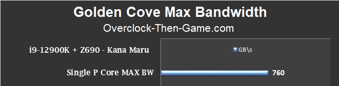
This shows a single Golden Cove under the best case scenarios that I could provide. The average BW was 760 GB\s which makes the Golden Cove blazing fast. The tests peaked at 1.07 TB\s which is amazing. The Golden Cove appears to be a serious performer and Intel’s 10nm is looking very good in this test.
Maximum Single “Gracemont” Performance

The best case scenario for a single Gracemont Core shows 283 GB\s on average. That’s not bad especially since there are 8 of them on the i9-12900K. The max performance peaked at 407 GB\s so there’s definitely some burst in performance under the correct workload scenarios.
Maximum Performance Cores vs Maximum Gracemont Cores
Now that we have seen the top performance single core results I will run all 8 Performance Cores against all 8 Efficient Cores. This test should allow maximum performance and latency should be fairly low. The goal is to test the actual cores while avoiding the L2 and L3 cache information.
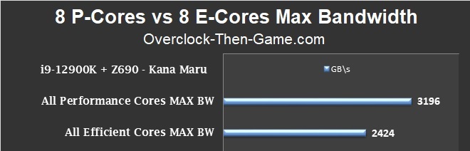
Starting with the Performance Cores first we can see that when all 8 cores are working together at the lowest level they can achieve some serious performance. Now we can see why Intel named them “Performance” cores. Under various workloads the average came out to 3,196 GB\s or in other words 3.2 Terabytes (T\Bs) a second. That is extremely high and the maximum performance topped out at 4.5 TB\s under specific workloads. Reading data is extremely fast and for data that only requires a single read and write, or data that isn’t dependent on other data, the Golder Coves moves tons of data very quickly. This is great to see as a former X58 1st Generation user. There have been many CPUs faster than my first gen, but I’m glad I decided to wait until Intel’s 10nm. Moving down to the “Gracemont” cores we see that all 8 Gracemont cores can move 2,424 GB\s on average, or 2.4 Terabytes (TB\s). This is incredible and goes to show how efficient and powerful the Gracemont cores really are when they are working together. Due to the low latency, being single-threaded and designed to produce high throughput the x8 Gracemont Cores can actually outperform the x8 Performance Cores in low latency situations that relies more on reading multiple lines of data. Earlier in the latency benchmark we saw that the Gracemont cores could access the L1 Cache 20% quicker than the Performance Cores. Well in a particular benchmark during this test the E-Cores showed a 79.2% increase over the Performance Cores. I’m sure it also helps that the Gracemont Cores are clustered as well. However, outside of that one scenario where the Efficient Cores outperform the Performance Cores, in another test the P-Cores make up for it with a 345% increase over the E-Cores. Overall when taking the average of all benchmarks performed in this test the Performance Cores are 32% faster than the Efficient Cores and of course specific tests can show much larger increases for both the Performance or the Efficient cores. Both cores have their strengths and weaknesses and so far I like what the benchmarks are showing me with Intel’s Hybrid Technology. Intel’s take on the big.LITTLE architecture seems to be a great move. Hopefully I was able to give more insight into the micro-architecture. Now we will move on to other higher level synthetic benchmarks.
Synthetic Benchmarks
Aida64 - Blender - y-cruncher - 7-zip
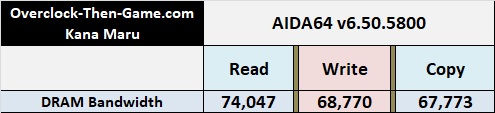
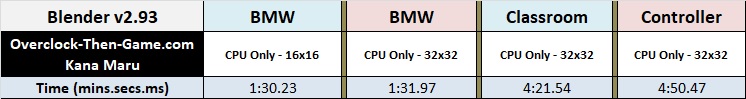
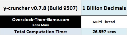
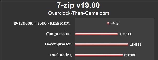
Now that we have a decent idea of how much performance we can expect from the Alder Lake micro-architecture; we will now take a look at several synthetic benchmarks to see how quickly the i9-12900K can complete various workloads. I would also like to add that AIDA64 cannot properly benchmark the Alder Lake CPU properly at the moment so I only posted the data that I could verify. I will need to re-visit the AIDA64 after the developers are able to update their software. Theoretically the Alder Lake micro-architecture along with my dual DDR5-4800Mhz DRAM should be able to reach 76,800 MB\s or 76.8 GB\s. Below you will see that AIDA64 obtained 74,047 MB\s or 74 GB\s which very close to theoretical max. However during my micro-architecture benchmarks I ran on the previous pages I was able to verify 75,672 MB\s or 75.7 GB\s. This puts the stock Alder Lake CPU and default DDR5-4800Mhz frequency extremely close to the theoretical bandwidth. However we must remember that latency can affect this number so 67GB\s though 74 GB\s might be normal under most workloads.
AIDA 64 v6.50.5800
Blender v2.93
y-cruncher v0.7.8 (Build 9507)
7-zip v19.00
Synthetic Benchmarks
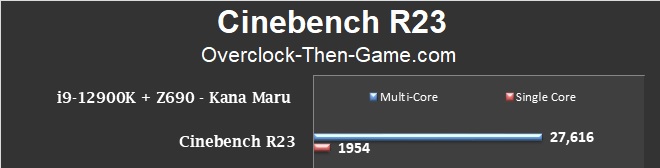
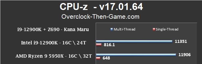
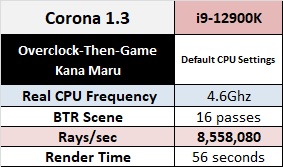
Cinebench R23 - CPU-Z - Corona
Cinebench R23
CPU-Z v17.01.64
CPU-Z included several CPUs as references
Corona 1.3
Synthetic Benchmarks
Google Octane, Kraken, WebXPRT 3
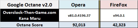
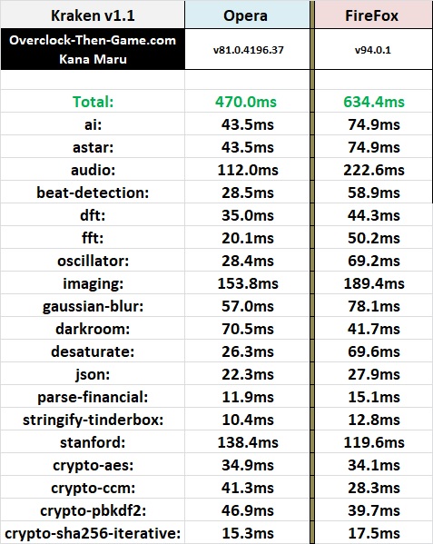
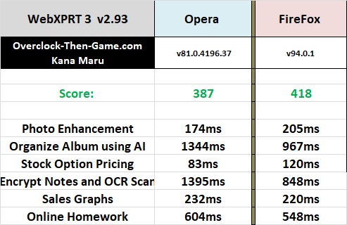
Now we can take a look at how well Alder Lake handles web-browsing performance.
Google Octane 2.0
Kraken v1.1
WebXPRT v2.93
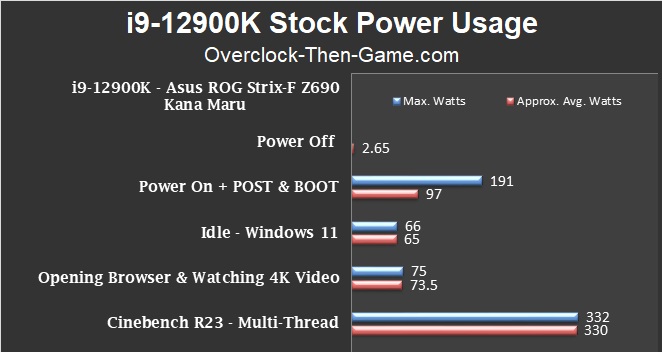
Power Consumption - Stock
Alder Lake Power Usage
On the chart below you will see that Alder Lake is very efficient for light workloads and idle periods. The chart below shows the total system wattage. The chart does not include additional wattage for a discrete GPU so only the CPU, RAM and Motherboard wattage is shown below. Light usage such as opening browsers, opening folders or apps shows that Alder Lake consumes roughly 74Watts. That number drops to 65Watts if the PC isn’t being used. While running Cinebench R23 the app ramps up the CPU utilization and the voltage. The system pulls 330Watts during the benchmark. The Alder Lake CPU itself only used approximately 214watts on average using software based monitoring.
Alder Lake CPU Temperature
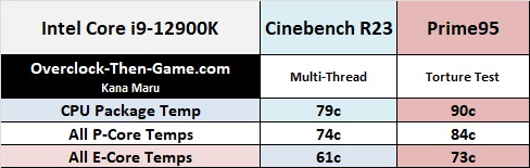
The CPU Package temperature showed an average of 79c in Cinebench R23. The peak temperature reached 81c. The CPU Package is overall temperature that we should pay attention to, but I also wanted to also show the average for all of the P-Cores and E-Cores as well. Only focusing on the P-Cores we see an average of 74c. The E-Cores shows an everage of 61c. For the record I am using a LGA1200 (Comet & Rocket Lake Socket) EK-360mm AIO CPU Cooler so if you have less than a 360mm radiator without powerful fans then your temps might be slightly higher. I am still waiting on the actual LGA1700 mounting bracket (Alder Lake Socket). Most users won’t run their CPU at 100% utilization most of the time and of course if the CPU becomes too warm Intel has built-in tech to throttle the performance. Intel tech will monitor the thermals and wattage to control the performance. There are many overclocking features to disable certain power wattage and thermal features so be careful and ensure that you have adequate cooling. To see how much of a beating the CPU AIO Liquid Cooled 360mm Radiator could take I decided to run Prime95’s torture test. The benchmark showed that the CPU temps averaged 90c and the peak temperature was 92c. Prime95 torture test is for extreme use only and stress testing the machine. It will never present a typical workload under normal circumstances. However, it was interesting to see the P-Cores increase by 10c and the E-Cores increase by 12c. Overall I feel that the 360mm AIO does a good job and unless you are planning to go for extremely high voltage overclocks you won’t have much to worry about. The limit for Alder Lake CPUs appears to 100c. At 100c the CPU will throttle and you will lose some performance. I am sure it is possible to disable this behavior, but I wouldn’t risk it if I were you.
Overclocking & OC Power Usage
Power Consumption - Alder Lake Overclocked
I haven’t had a lot of time to go through all of the overclocking settings in the UEFI menu. I have only had the i9-12900K for about 5 days at the time of this writing so the biggest bump in performance will be coming from the Efficient Cores. I know that is surprising, but I will explain. The stock i9-12900K runs at 4.9GHz for all P-Cores under heavy loads and 3.7GHz on the E-cores at stock settings. Overclocking Efficient cores were much easier than overclocking the Performance Cores. I was able to bump the P-Cores up slightly to 5.0GHz (+100Mhz \+2%) and the E-Cores up to 4.0GHz (+300Mhz \ +8%) over the stock settings. So while the Performance Cores barely increased and the Efficient Cores received a decent bump; we will now see how much of an increase we gain in both performance and power consumption.
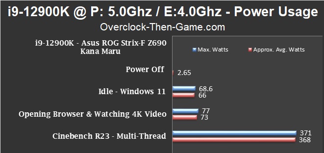
During idle periods and light usage the i9-12900K does a great job that is pretty much on par with the default stock settings. Looking at the Cinebench R23 results we can see an increase of approximately 36 watts on average over the stock settings. The maximum peak wattage increased by 41 watts. The temperature stayed roughly the same in Cinebench R23 (83c vs 79c) and Prime95 (95c vs 92c). You will definitely need top-notch cooling if you are planning to overclock the i9-12900K. It’s a good chance that you will hit the 100C limit and cause the CPU to throttle. However, as I stated earlier I’ll need more time with the Asus ROG Strix-F and Alder Lake CPU to get the most out of overclocking. So there should definitely be more overclocking articles coming soon. With that being said let’s see how the slight core frequency increase performs across several benchmarks.
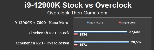
Cinebench R23 - Stock vs Overclocked
The multi-thread shows an increase of 3.6% and the single-thread shows an increase of 0.87%. I wasn’t expecting the single-thread score to increase that much since the Performance Cores frequency was only slight increased. The multi-score increase was nice though.
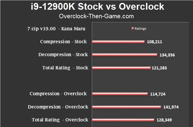
7-zip v19.00 - Stock vs Overclocked
In 7-zip we see decent performance increases during the compression & decompression tests. The Compression results increase by 6% and the Decompression improved by 6% as well. The overall Total Ratings increase was 5.82% or 6%. Not bad for a small and easy overclock.
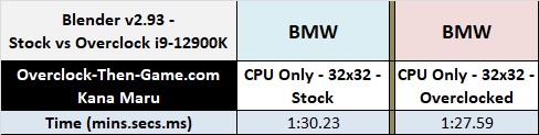
Blender v2.93 - Stock vs Overclocked
Blender shows a 3% increase. That’s small, but it could add up when you have many frames to render overtime. Most users will use either the GPU or both the CPU and GPU for rendering. This is something I plan to benchmark in the future with my RTX 3080 Ultra 240mm Liquid Coooled GPU.
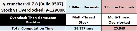
y-cruncher - Stock vs Overclocked
y-cruncher shows a 2% performance increase. Better than nothing I suppose.
Now that I have been able to compare several overclocked benchmarks against stock benchmarks one has to wonder if my slight overclock was really worth it. Well for some programs it could be worth it more than others. Overall you will see small performance increases with a small bump in frequency, but the power wattage increases as well as the temperature. For example you can expect roughly a 4.2% increase in performance, based on all of the programs that I benchmarked above, but that comes with a power wattage increase of about 10% on average when the CPU is being stressed @ 100%. The CPU temperatures will also play a part in this because you’ll want at least a 240mm\360mm or custom water cooling if you plan to overclock this CPU. On a more interesting note we will see what happens when I undervolt the Core i9-12900K while keeping the stock clocks on the next page.
Undervolting Alder Lake
There was a lot of concern about 12th Generation CPU power usage. The i9-12900K is rated to use up to 241watts, but typical use will be far below that. Microsoft’s Windows 11 along with the motherboard manufactures and Intel will have several ways to limit heat, wattage and performance for the best case scenarios, however I wanted to take matters into my own hands. As efficient as the 12th Gen is at low usage scenario’s I wondered if there was a way to make the maximum performance more efficient at stock frequencies. The stock frequencies for the P-Cores running at 100% loads are 4.9GHz and the E-Cores hit 3.7GHz. The frequencies are already very high, but even at stock it is possible to get more performance if the CPU thermals and voltages can be kept low. Intel uses “Thermal Velocity Boost” with the Alder Lake micro-architecture and this allows the CPU cores to increase their frequency if the CPU determines that the voltages and temperatures won’t cause the CPU to go out of spec. This will prevent high wattage, high heat and system instability. So my first goal was to see how much lower I could get the CPU voltage and wattage usage to drop. I was able to drop the CPU vCore from 1.26v to 1.16v with no problems. This showed some interesting results. The system stability appeared to be rock solid as it was able to complete many runs while using Cinebench R23 and Prime95’s torture test. So far it has passed every stability test I have thrown at it.
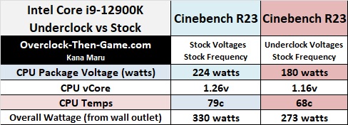
I captured some data from the Cinebench R23 runs and Alder Lake appears to very efficient. I’m not sure why Intel pushed the voltage so high, but so far I’m not running into any issues. The complete system only pulled 273 watts with 1.16v. That is much lower than the stock voltage (1.26v) that caused the system to pull 330 watts. I run my X58 with only 1.16v, but this on an old 1st Gen CPU and it is running at 3.8Ghz; Alder Lake is running 4.9Ghz(P) and 3.7Ghz(E). So right off the back I have cut down 57 watts while using the stock frequency. There was no drop in performance. I am allowing the motherboard and Windows 11 to control the fans speed and the fans are noticeably quieter. So it’s even possible to get lower temps if you wanted to ramp up the fans. During my tests I was able to drop the CPU temperature by 11C on average. The CPU Package voltage dropped by 44 watts which is great. Now the P-Cores can be as efficient as the E-Cores with much lower power. The E-Cores also become much more efficient. As I continue to learn more about the platform and begin to overclock different components I will definitely attempt to focus on optimizing my overclocks just as I have over the years with my X58 overclocks.
Conclusion

So we have reached the end of my Intel Core i9-12900K and overall I can say that it has been a pleasant surprise. Alder Lake has finally pulled me away from Intel’s 2008 X58 and so far it appears to be worth it. I skipped many generations from both Intel and AMD while enjoying gaming thanks to high-end GPUs from Nvidia and AMD. I went out of my way to avoid leaks, previews, reviews, YouTube videos and other outlets speaking about Alder Lake. I wanted the experience to be fresh and didn’t want to spoil the excitement. The Core i9-12900K packaging looks very nice and it is great to see companies being unique with their packaging nowadays. The overclocking features have been a nice surprise and there are tons of options for enthusiast to tweak in the UEFI. I will definitely be writing more articles regarding my overclocking results and other Alder Lake info that I discover. Overclocking the DDR5 should be fun as well.
Intel’s 12th Gen performance is great right out of the box and shows some impressive scores. Some software does not work properly or support Alder Lake’s new micro-architecture so we will have to wait for more developers to update their software. At that point we will be able to run more benchmarks. I was able to dive into the micro-architecture and gain more information that I was seeking. Getting this information wasn’t easy, but based on my tests I was able to extract some interesting information regarding the actual Performance Cores and Efficient Cores performance. I am still learning more about Intel’s new micro-architecture as well so if there were any mistakes I will be sure to update the article accordingly. Based on my results Alder Lake the micro-architecture appears to very good and can handle plenty of data.
Intel claims that the Performance Cores usage is for single-threaded and lightly threaded performance. I initially thought that the Efficient Cores would have higher latency than the Performance. However, during my deep dive into the micro-architecture it appears that the Performance Cores (75.4ns) seems to have much higher latency to DRAM access as opposed to the Efficient Cores (39.4ns). The P-Cores have SMT (Hyper-Threading) while the E-Cores doesn't support SMT (No HT). The Efficient Cores are clustered together in groups of four, share the same L2 Cache, but if each Cluster (x4-E-Cores + x1-L2 Cache) works on data independent of the opposite Cluster then both Clusters can independently output roughly 150 GB\s of data based on my benchmark testing. So the total could be 300 GB\s of data if the Windows 11 scheduler and Intel’s Thread Director can ensure data goes to the correct Efficient Cluster.
 With all that being said the Performance Cores are high-performance cores and the Efficient Cores live up to their name. Intel says that there are three separate fabrics, compute (1000 GB/s), memory (204 GB/s) and I\O (64GB/s) on the Alder Lake CPU. I was able to pull 713GB\s from all Cores (P & E) and if we add the other interconnects (Memory + I\O) that would put Alder Lake at 980 GB\s, just shy of that 1000 GB\s number that Intel claims. Intel does state “separate” and I am clearly combining them here so it’s possible that Alder Lake is capable of much more performance, but I will need more time to work with the new Intel Hybrid Technology. I’m just trying to make sense of it all. Nonetheless, I was very surprised at the actual individual single core performance from the Performance Cores and the Efficient Cores.
Taking a deep-dive into Alder Lakes micro-architecture was my favorite part this review, but there’s one other area that intrigued me even more and surprisingly it was not the overclocking, but the undervolting. While I do plan to overclocking Alder Lake in future articles I am left wondering why Intel pushed the wattage so high. I was able to undervolt the CPU voltage and practically make Intel’s Alder Lake extremely efficient across the board in every term that you can think of; CPU vCore, CPU Wattage, CPU Temperatures and overall wattage from the wall without losing any performance. This makes Alder Lake extremely useful for less extreme cooling solutions. If you are planning to overclock then you definitely want to ensure you have a good cooling solution, but at stock I was able to lower the voltage without losing stability. Alder Lake is more efficient than we thought and so far so good with lower voltage with no instability issues.
With all that being said the Performance Cores are high-performance cores and the Efficient Cores live up to their name. Intel says that there are three separate fabrics, compute (1000 GB/s), memory (204 GB/s) and I\O (64GB/s) on the Alder Lake CPU. I was able to pull 713GB\s from all Cores (P & E) and if we add the other interconnects (Memory + I\O) that would put Alder Lake at 980 GB\s, just shy of that 1000 GB\s number that Intel claims. Intel does state “separate” and I am clearly combining them here so it’s possible that Alder Lake is capable of much more performance, but I will need more time to work with the new Intel Hybrid Technology. I’m just trying to make sense of it all. Nonetheless, I was very surprised at the actual individual single core performance from the Performance Cores and the Efficient Cores.
Taking a deep-dive into Alder Lakes micro-architecture was my favorite part this review, but there’s one other area that intrigued me even more and surprisingly it was not the overclocking, but the undervolting. While I do plan to overclocking Alder Lake in future articles I am left wondering why Intel pushed the wattage so high. I was able to undervolt the CPU voltage and practically make Intel’s Alder Lake extremely efficient across the board in every term that you can think of; CPU vCore, CPU Wattage, CPU Temperatures and overall wattage from the wall without losing any performance. This makes Alder Lake extremely useful for less extreme cooling solutions. If you are planning to overclock then you definitely want to ensure you have a good cooling solution, but at stock I was able to lower the voltage without losing stability. Alder Lake is more efficient than we thought and so far so good with lower voltage with no instability issues.
Overall the Alder Lake release was smooth, but the OEMs did not have the LGA1700 CPU Coolers or brackets ready. I’m not sure if most of the blame should go to Intel or the manufactures. Luckily ASUS allows both LGA1700 & LGA1200 coolers to be used on their motherboards which was one of the strongest reasons I chose ASUS. Another reason I chose ASUS is because I have ran their ASUS Sabertooth X58 motherboard for well over a decade consistently with no issues. I am not sure how long I will be using the 12th Gen Alder Lake & Z690, but hopefully the same is true with their ASUS ROG Strix-F motherboard as well. Quickly, my thought on Windows 11 OS is that Microsoft is having another identity crisis. Microsoft does this every 4 to 6 years. Windows 11 is basically Windows 10, but the user interface reminds me of the 2005-2010 era Apple Mac UI. Certain features like separating windows are missing without editing the registry. The last time MS did something this drastic with the user interface was with Windows 8, but they got it right with Windows 10. The DDR5 RAM quickly sold-out and of course DDR5 came with a premium price for the new technology. I decided to purchase DDR5-4800Mhz to give a fair representation of the Alder Lake platform. The performance and bandwidth from the DDR5 RAM is great and I was able to pull a maximum of 75.6GB\s from my tests which puts me very close to my theoretical limit (76.8 GB\s). While I will be using Alder Lake + Z690 as my main workstation, I will still be using my X58 for various tasks that doesn’t require a lot of horsepower.
Long Live Bloomfield & Westmere + X58, but Alder Lake + Z690 has taken the crown in my home.
Thank you for reading my "Alder Lake-S Review" article. Feel free to leave a comment below and feel free to share this article. If you would like to see more content like this please consider donating to my Patreon or PayPal by clicking the images below. Thank you.