Intel's Z690 Chipset
Now that we have learned about Alder Lake’s microarchitecture and features we will switch the focus to the Z690 chipset. To support the high-speed coming to and from the CPU Intel has upgraded several key areas. To ensure that all of the new and fast technology has the required bandwidth Intel has updated their DMI 3.0 to DMI 4.0. DMI 4.0 is two times faster than DMI 3.0. Intel’s DMI 4.0 is the link between the Alder Lake CPU and the Z690 chipset and supports up to 8GB\s (bi-directional) so that comes out to 16GB\s. For comparison my 1st Generation X58 chipset used DMI 1.0 (QPI) which topped out at a blazing 2GB\s (bi-directional – 4GB\s) which makes DMI 4.0 four times faster than my X58 DMI\QPI link.
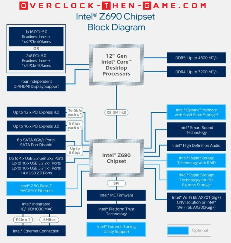
The Z690 Chipset supports PCIe 4.0 and 3.0. Intel states that the Z690 supports up to sixteen PCIe 4.0 connections running at x1 speeds (16 Gb\s) and up to 12 lanes. Motherboard manufactures will be combining these lanes and so far it appears that PCIe 4.0 running x8 mode (64 Gb\s) will be the standard for most PCIe connections. Many of the PCIe 4.0 lanes will more than likely mostly be used for M.2 SSD storage and other on-board features listed below. PCIe 3.0 will use up to 16 lanes. There are a ton of motherboards releasing with the Z690 chipset so there is no telling how many variations will be released over the next year or so. Intel’s Z690 Chipset is 14nm for those who might be wondering.
USB 3.2 (5Gb\s) and USB 3.2 (10Gb\s) are supported as well. Each USB 3.2 Gen ports (5Gb\s & 10Gb\s) will support up to 10 devices. USB 3.1 Gen 2 (20Gb\s) will support up to 4 devices. Although USB 3.x is backwards compatible USB 2.0 hasn’t gone anywhere. Intel will continue to support up to 14 USB 2.0 ports. Ethernet speeds of 1 Gbps will still be the standard, but the Z690 Chipset will natively support 2.5Gbps if the motherboard OEMs decide to support it as an option. 2.5Gbps will be overkill for most home users. Intel’s Optane Memory\Storage will be supported on the chipset as well. As far as RAID goes all of the standard RAID configurations (0, 1, 5, 10) will be allowed for both SATA and PCIe. Intel will allow native and discrete support for their Wi-Fi 6E. Intel’s Z690 chipset will allow OEMs to change many of the high-speed lanes. This is supported due to many different types of technology standards that the manufactures can specify as they see fit. Certain lanes won’t be changeable such as the DMI lanes or other reserved lanes, but other lanes, for instance PCIe 3.0 & 4.0, can be used for various purposes such as Gigabit Ethernet or 2.5Gb Ethernet, M.2 slots, SATA ports and so on. So for PCIe there is a maximum of 28 PCIe lanes, but only 12 PCIe 4.0 lanes are usable due to the other remaining 16 lanes being reserved for PCIe 3.0. For example a motherboard that I was viewing supports three PCIe 4.0 “M.2” slots in “x4 mode” which comes out to 12 lanes. This would leave that motherboard OEM left with 16 PCIe 3.0 lanes for various I\O ports (USB, Ethernet etc.) Obviously this will allow OEMs to create many tiers and SKUs for the Z690; all with different features and options.
12th Generation Overclocking
The last platform I have overclocked was the 2008 X58 platform that Intel released more than 13 years ago. There were many options and settings to tweak. It was a great and fun experience during that era. After the X58 platform overclocking on newer platforms started to be mostly reliant on overclocking the Voltage and CPU Ratio’s with various settings such as the Base Clock (BCLK) & PCIe Frequency being locked. I also understand why Intel decided to lock down certain frequencies as well, but the enthusiast platform has always been “High Risk – High Rewards”. Alder Lake and the Z690 Chipset have made me excited about overclocking again.